Download
1 / 25
250 likes | 321 Views
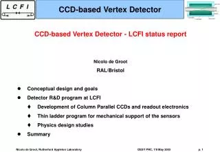
LCFI Collaboration Status Report. Steve Worm Rutherford Appleton Laboratory for the Linear Collider Flavour Identification (LCFI) Collaboration. Outline. LCFI activities Vertex software package Column-parallel CCDs: CPC2 Clock drive and CPC-T test structures Readout chip development

E N D
LCFI Collaboration Status Report Steve Worm Rutherford Appleton Laboratory for the Linear Collider Flavour Identification (LCFI) Collaboration
Outline • LCFI activities • Vertex software package • Column-parallel CCDs: CPC2 • Clock drive and CPC-T test structures • Readout chip development • ISIS developments and results • Mechanical studies
Vertex Package - Overview • Goals • Develop tools for the evaluation and optimisation of the vertex detector • Study benchmark processes; optimise the vertex detector • Package design overview • Vertex package interfaces to MarlinReco framework • Framework consists of software processors, enabled and configured via XML • Input: LCIO events • Processors: • Track selection cuts for ZVTOP, flavour tag, vertex charge • IP fit processor • ZVRES • ZVKIN • Output: dedicated vertex class in LCIO format, with vertex information, flavour tag inputs, NN flavour tag output and vertex charge Big step towards full MC simulation and reconstruction (MOKKA+MarlinReco) • Jet flavour MC truth information • Calculation of NN input variables • Training NN for flavour tag • NN outputs from trained nets • PlotProcessor for standard plots
Vertex Package - Comparisons • Example plots: Purity vs. Efficiency • Compares well with SLD/Fortran algorithm • Analysis at Z-peak energy with fast MC (left) and full Geant4 MC (right) • Excellent agreement with fast MC (identical inputs) • Very good agreement also with full MC (dependant on tracking input chosen) b c (b-bkgr) c Filled: LCFI (c++, MARLIN, fast MC) Open: previous (Fortran, fast MC) Filled: LCFI (c++, MARLIN, MOKKA full MC) Open: previous (Fortran, Brahms full MC) E. Devetak, M. Grimes, S. Hillert, B. Jeffery
LCFI code FORTRAN LCFI code FORTRAN Vertex Package - Comparisons • Joint probability and PT-corrected vertex mass • Shown are the two most important flavour tag inputs • Excellent agreement between LCFI code and Fortran result • Details in recent LC Note
Vertex Package - Verification and Status • Verification Procedures and Results • Stage 1: Comparisons between SGV and MARLIN using identical inputs • Stage 2: Same events passed through full MC simulation in MOKKA • Grid sample creation and MarlinReco debug in collab with MPI Munich, DESY • Compare MARLIN (MOKKA input), MARLIN (SGV input), and BRAHMS (TESLA TDR) • Profiling with Valgrind to check for memory leaks, improve performance • Preliminary results:MARLIN (c++) slightly outperforms SGV (Fortran) • Status • Fully functional, ~20,000 lines of c++ code • Released ~two weeks ago; available from the ILC software portal • Considered a ‘highlight’ of the ILC Software Workshop (2-4 May) • After release • Tutorials for new users (starting soon) • Move to full tracking (currently use simplified tracking “cheaters”) • Move to more realistic vertex detector geometry (ladders, not cylinders) • Further optimisation of cuts, parameters and algorithms Huge effort, and now available for use!
ILC Vertex Detector Requirements • Excellent point resolution • Small pixels: ie 20 μm x 20 μm • Close to the IP: inner radius ~1.5 cm • Fast (low ocupancy) readout • Column-parallel CCD: readout during 1 ms beam at 50 MHz (inner layer) • In-situ Storage Image Sensor (ISIS): storage of data for readout in long (~200 ms) inter-train gaps • Extremely small material budget • ~0.1% X0 per layer --> low power dissipation • Overall detector geometry • Sensor+layout concept actively being developed • Pixels in 5 layers, ~109 channels
Column Parallel CCD Readout time = N/Fout M N N “Classic CCD” Readout time NM/Fout Column-Parallel CCDs • Fast Column-parallel CCDs (CPCCD) • CCD technology proven at SLD, but ILC sensors must be faster, more rad-hard • Readout in parallel addresses speed concerns • CPCCD’s feature small pixels, can be thinned, large area, and are fast • CPC1: two-phase, 400 (V) x 750 (H) pixels, each 20 20 μm2 Bump-Bonded CPCCD + Readout CPCCD1
First-generation tests (CPC1): Noise ~100 e- (60 e- after filter). Minimum clock potential ~1.9 V. Max clock frequency above 25 MHz (design 1 MHz). Limitation caused by clock skew Next generation now available (CPC2): Busline free design (two-level metal) Large area ‘stitched’ sensor, choice of epi layers for varying depletion depth Range of device sizes for test of clock propagation (up to 50 MHz) Large chips are nearly the right size Level 1 metal Polyimide Level 2 metal Φ2Φ1 CPC2 Wafer Column-Parallel CCDs: CPC1 results and CPC2 design CPC2-70 9.2 cm
ISIS test structures CPC2-70 CPC2-40 CPC2-10 CPC2: Next generation CCD • CPC2: second generation Column-parallel CCD • Single-metal: (100 Ωcm @ 25 µm and 1.5 kΩcm @ 50 µm) • 2 more wafers received with 2-level metal (busline-free) • Busline-free variant designed for 50 MHz operation • Another 10 wafers in pipeline Busline-free design a big step! Busline-free CPC2
Busline-Free CPC2 - First Results • First test results from high-speed, double-metal CPC2-10 • Clear X-ray hits at up to 45 MHz despite significant clock feed-through • Transformer drive (shown) is challenging due to numerous parasitics Major result for LCFI (but that’s not all)… 55Fe source removed X-ray hits CCD output (2-stage source follower), ~2 Vpk-pk clocks
Busline-Free CPC2 - First Results • Works at very low clock amplitude • Clock amplitude for plot below is only 0.4 Vpk-pk • Significant noise induced from clock • Low clock due to very low dose inter-gate implant (not a resonance effect) • Further tests to use CMOS-based drive chip (CPD1)
T. Woolliscroft 55Fe signal CPC2+CPR2 Hybrid Assemblies • Tests on bump-bonded assemblies have started • Two wafers-worth of bonded assemblies received • First response to X-rays observed (below) • Not all has gone smoothly…
Cs Cs Phase1 Phase1 2Cig Cig 2Cig Phase2 Cs Phase2 Cs Capacitance Reduction Ideas for CCDs • High capacitance CCD is challenging to drive • 40 nF and ~2V clocks @ 50 MHz… >20 amps! • Working to reduce capacitance (and drive voltage) • Inter-gate capacitance (Cig) is dominant; depends on gate and overlap sizes • New sensor designs (open phase, pedestal gate, and shaped channel) can reduce Cig by factor of ~4? New test structure to test these designs - production starting at e2v Open phase CCD
Transformer-based driver Designed for 2 Vpeak-to-peak at 50 MHz and 40 nF (ie for CPC2-40) Planar air-core transformers on 10 layer PCB, 1 cm2 Parasitic capacitance and inductance of bond wires a major effect Works with “busline-free” CPC2 CPD1 driver ASIC Designed for either large or small sensors: 40 nF/phase at 50 MHz or 127 nF/phase at 25 MHz One chip drives both phases with 3.3V clock swing, 21 amps/phase 0.35m CMOS process, 3x8 mm2 Clock drive for CPC2 Transformers CPD1
CPD1 Driver ASIC Slew rate in slow mode Rise time: 50ns, 2s, 4s CPD1 works well! • Features • Three separate modes for operation over a wide range of frequencies • Bias circuitry, local decoupling capacitance, control logic • Designed to provide >2V peak-to-peak at up to 50MHz • Testing results • Control circuitry works fine • Integrated capacitive load works well • Tested in package (inductance limited) • Full testing started in dedicated board; internal (2 nF) and external (40 nF) loads 2nF load, Fast Mode, 25 MHz PH1 PH2 PH1-Ph2
Readout Electronics: CPR2 Readout Chip • Designed to match the Column Parallel CCD (CPC2) • 20µm pitch, maximum rate of 50MHz • 5-bit flash ADC, on-chip cluster finding • Charge and voltage inputs • Features for the CPR2 include • Cluster Finding logic, Sparse read-out • Better uniformity and linearity • Reduced sensitivity to clock timing • Digital and analogue test I/O • Variety of test modes possible • 9.5 mm x 6 mm die size, IBM 0.25µm Major piece needed for a full module
CPR2a Readout ASIC • CPR2 Readout ASIC: Works, but deadtime and some data loss for large clusters • CPR2a Readout ASIC: • Pad-compatible, but with significant changes to digital • Implemented features: Increased front-end memory depth, clustering now 4x6, compact layout, no repetition of time stamp, per-column threshold • Next steps: Flag for corrupt or lost data, more digital outputs, optimisation of analogue stages
Reset transistor Source follower Row select transistor sense node (n+) reset gate row select to column load VDD storage pixel #1 storage pixel #20 output gate transfer gate photogate n+ buried channel (n) p+ well p+ shielding implant reflected charge Charge collection reflected charge substrate (p+) High resistivity epitaxial layer (p) In-Situ Storage Image Sensor • ISIS Sensor details: • CCD-like charge storage cells in each pixel, CMOS or CCD technology • p+ shielding implant (or epi) forms reflective barrier • Operational Principles: • Charge collected at photogate, transferred to storage pixel during bunch train • 20 transfers per 1 ms bunch train • Readout during 200 ms quiet period after bunch train
5 μm Global Photogate and Transfer gate ROW 1: CCD clocks ROW 2: CCD clocks On-chip switches On-chip logic ROW 3: CCD clocks ROW 1: RSEL Global RG, RD, OD RG RD OD RSEL Column transistor ISIS Properties and Status • ISIS advantages: • Low frequency clock -> easy to drive • 20 kHz during capture, 1MHz readout • ≈100 times more radiation hard (fewer charge transfers) • More robust to beam-induced RF pickup • Process and Status: • Combines CCD and active pixel technologies • Deep implant or custom epi needed • Investigating CMOS and CCD vendors Proof of principle device (ISIS1) manufactured
The ISIS1 Cell • Array and Cell details • 16x16 array of ISIS cells with 5-pixel buried channel CCD storage register • Cell pitch 40 µm x 160 µm • No edge logic (pure CCD) • Chip size 6.5 mm x 6.5 mm Output and reset transistors OG RG OD RSEL Column transistor OUT Photogate aperture (8 μm square) CCD (5x6.75 μm pixels)
Radiation Damage Effects in CCDs • Simulation of Charge Transfer • Full 2D simulation in ISE-TCAD • Count signal e- trapped in pixel • CPU-intensive and time consuming • Simple analytical model gives similar results • Window of low charge transfer inefficiency (CTI) between -40 °C and 0 °C for 50 MHz Very important for operation… must confirm with data! -0.17eV trap -0.44eV trap
Ladder Prototyping • Ultra-low mass ladders a significant challenge • 0.1% X0 per layer: active silicon sensor thickness and not much else! • Low power, low flow rate gas cooling only • Foam structures being investigated • Low mass, good rigidity • Silicon+foam or Si+foam+Si sandwich • Good thermal match for SiC and RVC • Silicon Carbide (SiC) • SiC as ladder support looks promising • Built 8% SiC on 25 μm Si 0.16 X0 • 0.1 X0 possible with ~5% foam • Ladder profiles with small T steps look good (see plots at right) • Reticulated Vitreous Carbon (RVC) • RVC ladder currently under test • ~3% foam and 2x25μm Si ~0.1 X0 • Sandwiched structure for rigidity
cooling inlets heater elements Cooling Studies • Goals • Develop design capability- a predictive tool, not for layout optimisation • Gas cooling test stand • Major update with Perspex (insulating) ladders and end plates now complete • Data collection underway with upgraded software • Simulation of test stand • Upgraded software, computing power • New CFD model includes solid domain • Still optimising inlets, heater elements
Conclusions • Physics Studies • Vertex package released and available for public • Important for ILC vertex-related physics studies • Column-parallel CCD • Second generation high speed CCD: CPC2 working at 45 MHz • Active programme of capacitance and clock amplitude reduction • Clock driver under development (CMOS and transformer) • Third-generation readout ASIC available, new one under design • In-situ Storage Image Sensor • Proof of principle device works • Design of small-pixel ISIS2 in progress • Mechanical Studies • Active programme of ladder mechanical prototyping • Cooling test stand and simulation work converging LCFI making excellent progress towards meeting the challenges of the ILC