Download
1 / 22
230 likes | 432 Views
ON-CHIP SCANNING CONFOCAL MICROSCOPE WITH 3D MEMS SCANNER AND VCSEL FEEDBACK DETECTION C. Gorecki , L. Nieradko et. al. Université de Franche-Comté, Besançon, FRANCE Wroclaw University of Technology, Wroclaw, Poland Transducers 07’ p 2561~2564. Reported by: Institute : 奈微所

E N D
ON-CHIP SCANNING CONFOCAL MICROSCOPE WITH 3D MEMS SCANNER AND VCSEL FEEDBACK DETECTION C. Gorecki, L. Nieradko et. al. Université de Franche-Comté, Besançon, FRANCE Wroclaw University of Technology, Wroclaw, Poland Transducers 07’ p 2561~2564 Reported by: Institute : 奈微所 Name : 楊志誠 Student ID: d9635804 VCSEL (Vertical Cavity Surface Emitting Lasers)
Outline • Introduction • Design and Fabrication • Experimental & Simulation Results • Conclusion
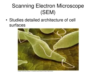
Microscope History 虎克發明光學顯微鏡 賓尼等人發明STM, AFM 1665 1886 2007 1981~1986 蔡司改良鏡片技術光學顯微鏡從此性能高強價格低廉 Now MEMS 1950 年代 TEM SEM 1957 Marvin 發明Confocal TEM的電子束要能穿透切成薄片的標本, 通常用來研究細胞內部的超顯微結構 SEM 標本的表面先鍍上薄薄的一層黃金, 再用電子束掃瞄其表面,適合用來研究標本表面的微細結構 ,通常可以拍攝同一細胞表面的3D立體結構
Scanning Confocal Microscope • Widely used in biomedicine, living cell • Three-dimensional (3-D) image • Non-invasive imaging of transparent samples 1.Reject light from out-of-focus planes 2.Provide clear in-focus image of a thin cross section http://www.microscopyu.com
Introduction • Design and Fabrication • Experimental & Simulation Results • Conclusion
ARCHITECTURE OF CHIP-SCALE CONFOCAL MICROSCOPE • 3 layers structure • Comb-drive actuators (Z and X-Y) • 100 μm for Vertical motion (Z) • 50 μm in both directions by • actuating of micro lens by x-y-axis • scanner • . • Laser microscope on-chip • silicon-based MEMS • Glass micro lenses • . VCSELs (Vertical Cavity Surface Emitting Lasers)
Fabrication process of glass microlens.[ Method 1] Isentropic Etching Glass reflow DRIE
Fabrication process of glass microlens [ Method 2] • single-mask process • KOH water solution<111> <100> Single-mask microfabrication of aspherical optics using KOH anisotropic etching of Si
Introduction • Design and Fabrication • Experimental & Simulation Results • Conclusion
ANSYS Simulation • Different shape design to investigate their performance • Frequency and vibration [ High Displacement & Lower voltage ] [Higher Rigidity & Higher voltage ] for lens D > 300 μm
Glass microlens fabrication • The silicon mould having depth from 46 μm to 90 μm • Etch depth is non-linear function of mask diameter • Etch rate 1.0-2.0 μm/min • Mask Diameter & Mould Diameter are linear • larger Microlens focal length • Increased Etched time • Silicon Nitride thicker
Introduction • Design and Fabrication • Experimental & SimulationResults • Conclusion
Conclusion • Precise positioning and focal tuning of micro lens • — 2-3μm resolution • — penetration depth down to 30 μ m • Achieved high-resolution positioning control without need for large numbers of electrodes — 50 μm (X,Y) — 100 μm (Z) • 500 times smaller than anything in this class
Discussion • Wavelength of light used is major factor in resolution • shorter wavelength greater resolution • Rayleigh criteria refractive wavelength shorter,the penetration depth will be shallow。 • Cell Damage: Cell damage and death for laser light • Bleach:Most specimen without fluorescent,so adding dyes are necessary。 • Laser light will bleach the dyes in the period of lighting。
Reference [1] .Magnetically Actuated Scanning Microlens for NIR Raman Spectroscope , Chin-Pang- Billy Siu et al, MEMS 2007, Kobe , Japan, pp 735-738 [2]. S. Kwon and L.P. Lee, “Micromachined transmissive scanning confocal icroscope”, Optics Lett, vol. 29, pp. 706-709, 2004. [3] S Bargiel, L Nieradko, M Józwik, C Gorecki, J.A Dziuban, “New generation of fully integrated optical microscopes on-chip: application to confocal microscope“, Proc. SPIE, vol. 6186, 2006. [4] D. Heinis, C. Gorecki, “Feedback-induced voltage change of Vertical Cavity Surface Emitting Laser as an active detection system for miniature optical scanning probe microscopes”, Optics Express, vol. 14, pp. 3396-3405, 2006. [5] R. Carrasco, J.A. Dziuban, I. Moreno, C. Gorecki, R. Walczak, M. Kopytko, L. Nieradko, M. Józwik, “Optical microlenses for MOEMS” Proc. SPIE, vol. 5836, pp. 657-666, 2005. [6].http://www.cyto.purdue.edu/flowcyt/educate/pptslide.htm [7]. www.cs.uky.edu/~jzhang/CS689/chapter7.pdf [8]. http://www.ntrc.itri.org.tw/dict/content.jsp
Vertical cavity surface emitted laser 面射型雷射二極體為一新型發光元件,此元件與傳統雷射二極體基本的差別在於 共振腔 磊晶層相對位置之不同;傳統雷射二極體的共振腔與磊晶層平行,反射面 係利用晶體自然斷裂面形成而與磊晶層垂直,雷射光由側面發出,故又稱邊射型雷射 (Edge-emitting laser),而本元件的共振腔與磊晶層垂直,反射面係由磊晶層或表層 介電質薄膜組成,雷射光由正面發出,故稱為垂直共振腔面射型雷射。 邊射型雷射於晶片製程結束後須將晶片劈裂成晶條,並進行端面鍍膜,此製程複雜 耗時且為影響製程良率之關鍵。面射型雷射因非利用晶體自然斷裂面作為反射面,故 無須利用劈裂或進行端面鍍膜,可節省可觀之製程時間並避免因此而影響製程良率。 另於晶片製程結束後即可於晶片上直接進行元件量測(on wafer testing),可節省量測 成本及時間。 預期面射型雷射可能之應用方向有下列各項:‧光數據鏈路傳輸(Serial Optical Data Links)目前已有HP、Motorola、Honeywell、 IBM、Vixel等公司投入 ‧雷射列印(Laser Printing):利用面射型雷射則可同時二維列印,加快列印時間, 目前Xerox已投入此方面研究。 [工 業技術研究院 奈米科技研發中心] http://www.ntrc.itri.org.tw/dict/content.jsp
θ Rayleigh Criterion Definitions • Acceptance angle θ • Numerical Aperture NA = n sinθ • Rayleigh resolution criterion for • a circular aperture Δx = 0.61 λ/NA • Highest Typical Resolution • Optical Microscope ~200 nm • Electron Microscope ~0.1 nm
Confocal Characteristics TranditionalConfocal Horizontal resolution (diffraction limited): Vertical resolution 共焦掃描顯微鏡僅對在聚焦面上形成清晰的影像,若我們逐步移動聚焦面,則可取得觀測樣品其深淺有序的斷面,將這些斷面的影像經由電腦處理,即可重組出相對應的三度空間影像。
Zeiss 510 Zeiss Confocal Microscope
Sources of Aberrations • Monochromatic Aberrations • Spherical aberration • Coma • Astigmatism • Flatness of field • Distortion • Chromatic Aberrations • Longitudinal aberration • Lateral aberration Images reproduced from: http://micro.magnet.fsu.edu/