Download
1 / 14
140 likes | 306 Views
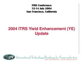
ITRS Conference July 14 - 16, 2003 San Francisco, California 2003 ITRS Yield Enhancement (YE) Update. Fred Lakhani 512/356-7011 fred.lakhani@sematech.org. Yield Enhancement Presentation Outline. ITWG Co-chairs and Contributors Chapter Outline Definition and Scope Difficult Challenges

E N D
ITRS Conference July 14 - 16, 2003 San Francisco, California 2003 ITRSYield Enhancement (YE) Update Fred Lakhani 512/356-7011 fred.lakhani@sematech.org
Yield Enhancement Presentation Outline • ITWG Co-chairs and Contributors • Chapter Outline • Definition and Scope • Difficult Challenges • Technology Requirements and Potential Solutions • Yield Model and Defect Budget (YMDB) • Defect Detection and Characterization (DDC) • Yield Learning (YL) • Wafer Environment Contamination Control (WECC) • Summary
Taiwan Tings Wang Promos Technologies Len Mei Promos Technologies United States Fred Lakhani International Sematech Christopher Long IBM 2003 ITRS YE ITWG Co-chairs • Europe • Ines Thurner • Infineon • Dick Verkleij • fei • Japan • Masahiko Ikeno • Renesas • Hiroshi Kitajima • Selete • Korea • TBD Note: Contributions of all TWG members around the world are gratefully acknowledged.
Europe Ines Thurner (Infineon) Dick Verkleij (fei) Lothar Pfitzner (FhG-IISB) Andreas Nutsch (FhG-IISB) Andreas Neuber (M+W Zander) Hans-Martin Dudenhausen (isiltec) Japan Masahiko Ikeno (Renesas) Hiroshi Kitajima (Selete) Toshihiko Osada (Fujitsu) Taiwan Tings Wang (Promos Tech) Len Mei (Promos Tech) United States Fred Lakhani (ISMT) Christopher Long (IBM) Mike Patterson (Intel) Kevin Pate (Intel) Mike Retersdorf (AMD) Ron Remke (ISMT) Mike McIntyre (AMD) Rick Jarvis (AMD) Ken Tobin (ORNL) Hank Walker (Texas A&M) Charles Weber (Portland State Univ.) Ralph Richardson (Air Products) Mark Camenzind (Air Liquide) Joe O’Sullivan (Intel) John DeGenova (TI) Jeff Chapman (IBM) Val Stradzs (Intel) Keith Kerwin (TI) James McAndrew (Air Liquide) 2003 YE ITWG Contributors
Yield Enhancement Chapter Outline • Definition and Scope • Difficult Challenges • Technology Requirements and Potential Solutions • Yield Model and Defect Budget (YMDB) • Defect Detection and Characterization (DDC) • Yield Learning (YL) • Wafer Environment Contamination Control (WECC)
Yield Enhancement Definition and Scope • Definition: • To improve the baseline yield for a given technology node from R&D yield level to mature yield. • The definition assumes a functional baseline process for a given process technology and it’s compatibility with the design of the product being fabricated. • The definition reinforces the chapter focus on the yield ramp portion of the yield learning curve. • Scope • Limit scope of YE chapter to wafer sort yield. • Fab line yield, assembly/packaging yield and final test yield are not included in the scope of the YE chapter.
YE Difficult Challenges • High-Aspect-Ratio Inspection. • High-speed, cost-effective tools are needed to rapidly detect defects at 1/2 X ground rule (GR) associated with high-aspect-ratio contacts, vias, and trenches and especially defects near or at the bottoms of these features. • Non-visual Defect Detection • In-line and end-of-line tools and techniques are needed to detect non-visual defects. • Design for Manufacture & Test (DFM & DFT) and Systematic Mechanisms Limited Yield (SMLY) • IC designs must be optimized for a given process capability and must be testable and diagnosable. Understanding SMLY is mandatory for achieving historic yield ramps in the future.
Canal Upper Dielectric Hard Mask Via Dielectric CMP Barrier Via Etch Barrier Lower Dielectric Canal Etch Barrier A B C D High-Aspect Ratio Inspection (HARI) Void caused by residue left behind after via etch process step
YE Difficult Challenges (continue) • Data Management for Rapid Yield Learning. • Automated, intelligent analysis and reduction algorithms that correlate facility, design, process, test, and work-in-process (WIP) data must be developed to enable the rapid root-cause analysis of yield-limiting conditions. • Yield Models • Random, systematic, parametric, and memory redundancy models must be developed and validated to correlate process-induced defects (PID), particle counts per wafer pass (PWP), and in-situ tool/process measurements to yield. • Correlation of Impurity Level to Yield. • Data, test structures and methods are needed for correlating fluid/gas contamination types and levels to yield.
YE Difficult Challenges (continue) • Line edge roughness, ACLV, subtle process variation. Where does process variation stop and defect start? Need to improve signal to noise to delineate defect from process variation. • Contamination transferred from wafer edge and backside. • Unified definition of defects based on yield impact.
AEA (knowledge discovery) SPC SSA ADC • optical • confocal • SEM • FIB Yield Management engineering analysis process data management system product data management system WIP data management system Databases ... fabrication process A fabrication process B assembly & final test bin, bit, and parametric electrical test data in-line optical defect data tool state, ISPM, moisture, etc. tool state, ISPM, moisture, etc. Yield Management TodayIncreasing Data Complexity
Technology Requirements and Potential Solutions • Yield Model and Defect Budgets • With systematic mechanisms limited yield (SMLY) dominating the rate of yield learning, a concerted effort is required to understand, model and eliminate SMLY detractors. • The impact of line edge roughness (LER) on yield needs to be understood, modeled and controlled to achieve acceptable yields for current and future technology nodes. • Continuous improvement in tool cleanliness will be required to achieve acceptable yields. • Defect Detection and Characterization • Cost effective high throughput high aspect ratio inspection (HARI) tools are needed urgently to achieve acceptable yields for current and future process technology nodes. • Signal to noise improvements are required for defect metrology tools to detect ever shrinking critical defects of interest.
Technology Requirements and Potential Solutions…continue • Yield Learning • With increasing process complexity and longer cycle times, tools and methods are needed to increase the number of yield learning cycles for each technology node. • With move to smaller features, longer processes, 300mm wafers and new materials (low k, high k, etc.), numerous tools and methods are required to understand all the yield detracting interactions. Use of SOI and SiGe will further challenge yield learning. • Wafer Environment Contamination Control • Data, test structures and methods are needed to identify and control yield detracting contaminants in the wafer environment, airborne and process critical materials and ultra pure water.
Summary • The YE chapter revision for the 2003 ITRS roadmap is well under way. The following regions are taking the lead in revising various sections of the YE chapter: • Yield Model and Defect Budget Japan • Defect Detection and Characterization Europe • Yield Learning USA • Wafer Environment Contamination Control USA • Yield critical small defects, high aspect ratio defects, non-visual defects and systematic mechanisms limited yield (SMLY) top the list of challenges for Yield Enhancement. • The yield enhancement community is constantly challenged to achieve acceptable yield ramp and mature yields due to increasing process complexity and fewer yield learning cycles with each subsequent technology node.