STM
STM. Scanning Tunneling Microscope Introductory Material Developed by Malory M. Peterson, Summer 2006 Nanotechnology Grant National Science Foundation #0532516. SPM – Scanning Probe Microscopy. There are two types of SPM AFM – Atomic Force Microscopy STM – Scanning Tunneling Microscopy

STM
E N D
Presentation Transcript
STM Scanning Tunneling Microscope Introductory Material Developed by Malory M. Peterson, Summer 2006 Nanotechnology Grant National Science Foundation #0532516
SPM – Scanning Probe Microscopy • There are two types of SPM • AFM – Atomic Force Microscopy • STM – Scanning Tunneling Microscopy • This unit focuses on the STM • SPM is used to image and learn more about the following: • Solid surfaces • Metal surfaces (roughness) • Modify surfaces • Surface adsorption (metals, minerals) • Surface manipulation by STM/AFM • Surface characterization • Thin-film technology • Semiconductors • Optical and compact discs • Bonding characteristics
New Research - STM The 1986 Nobel Prize in Physics was awarded for STM contributions – Information from the Nobel Prize Foundation ~ Nobelprize.org
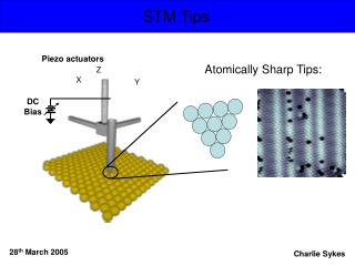
The STM is an Electron Microscope • When imaging atoms, an electron beam has to be used, because light waves are too large to detect objects that small. • Electron microscopes use beams of electrons, instead of light, to illuminate an object. • The tip of the STM is a very sharp point. It must be as small as possible in order for there to be a build-up of electrical charge. This will encourage electron tunneling between tip and surface. • The goal is to have the tip be the size of a single atom. • The tip is placed very close to the sample, but it does not touch the sample.
STM Scans • The sample MUST be conductive. • A small voltage is applied to the system. This allows electrons to tunnel between the tip and the sample. The tunneling electrons create an electric current. • The electric current is read on a logarithmic scale. Whenever the distance between the sample and the tip increases by 1nm the current can increase by about an order of magnitude (or x10). • In the picture on the right, the current will be much stronger between the light blue atoms and the tip, than between the dark blue atoms and the tip. • The current is measured and translated to form a topographical map.