Download
1 / 32
320 likes | 344 Views
Explore the evolution of chip embedding technology, process overview, applications, and conclusions from interconnect evolution to µVias and LDI. Discover the progress from 1970 to 2010. Learn about the HERMES Project advancements in embedding chips for reduced size modules and electronic systems.

E N D
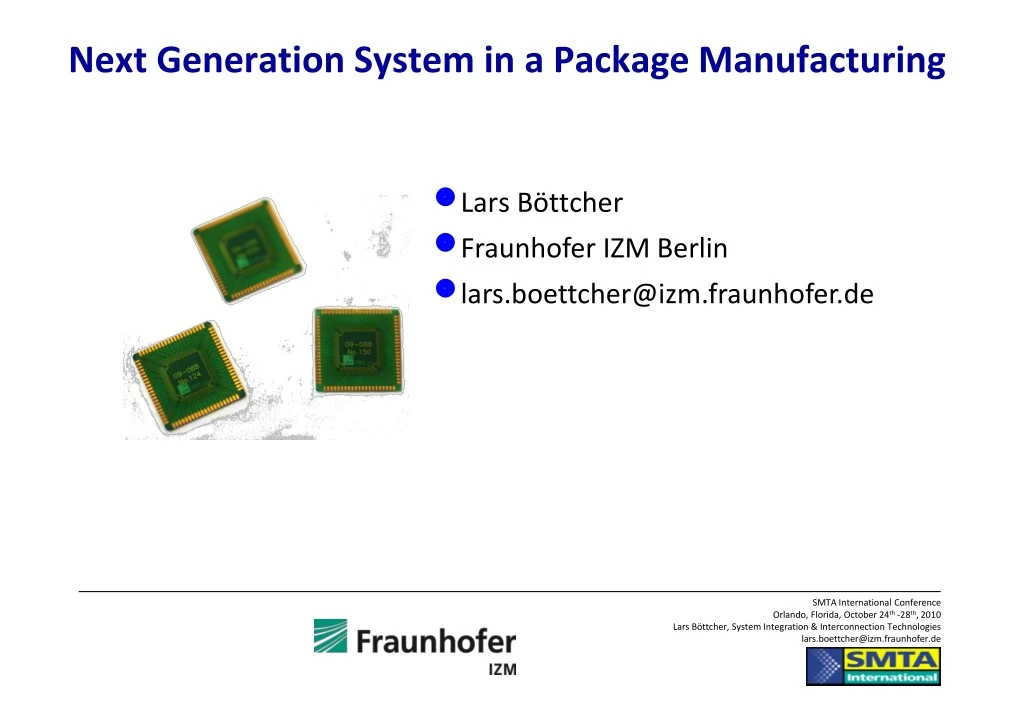
Next Generation System in a Package Manufacturing • Lars Böttcher • FraunhoferIZM Berlin • lars.boettcher@izm.fraunhofer.de
Outline • Introduction to Chip Embedding Technology • HERMES Project • Technology • Process overview • QFN Package realization • Ultra fine line • Ultra Fine pitch • Applications • Conclusions
Interconnect Evolution µVias LDI Embedding HDI PCBs technology challenge / potential Flip Chip progress of organic substrates enabled advance in interconnect technology chip & wire 1970 1990 2010
Chip Embedding - Technology Progress Chip Embedding in organic substrates use of PCB technology & material • Production started • Korea • Japan • First Standard • JPCA • EU Companies • ready Basic R&D Production Demos Production First Patent 2005 2010 2000 1968
Chip Embedding - Different Approaches Chip Last / Pad Connection Chip First / Via Connection core assembly embedding • use of pre-tested cores • different interconnect technologies (wires, solder, adhesives) • contact by micro vias • chip assembly in PCB flow • highest possible miniaturization pictures: Shibata, JPCA
Chip First Embedding - Process Alternatives Face Up Face Down die placement embedding via formation plating & etch electrical and thermal backside contact better fine pitch capability
HERMES High Density Integration by Embedding Chips for Reduced Size Modules and Electronic Systems Please visit: www.hermes-ect.net for more information • Project • EU funded project, FP 7 program, Started: May 2008, Duration: 36 month • Total budget (approx.): 16 M€ • Project Goal • Industrialization of the results of the HIDING DIES project • Improvement of technology towards finer pitch, use of new material developments, process innovation and equipment improvements • Strong focus on future implementing of the technology in a manufacturing environment / assembly chain • Consortium • 11 partner; technology provider, end-user, testing, research institutes • Early Adopters Group with potential end-users
HERMES – Technology Development Roadmap • Industrialization Goals • manufacturing panel size 18"x24" • lines/spaces 25 µm, semi-additive technology • die pitch 125 µm peripheral, 250 µm area array • stacking of 2 levels with embedded chips • Demonstrator Applications • Power module for house hold (4 ICs, large power dissipation) • Communication modem (> 10 ICs, high complexity) • Motor control unit (high-end micro controllers) • Secure phone module • Advanced Technology Goals • lines/spaces 15 µm, semi-additive technology • die pitch 60 µm • stacking of 2 levels with embedded chips
Outline • Introduction to Chip Embedding Technology • HERMES Project • Technology • Process overview • QFN Package realization • Ultra fine line • Ultra Fine pitch • Applications • Conclusions
Process Flow Face-Up Embedding • Panel format 610 x 456 mm² • 50 µm chips with 5 µm Cu or Ni/Pd pad metallization • Die attach (Dataconevo/Siplace CA3) using 20 µm DDAF (dicing die attach film) • Embedding (Lauffer) by RCC lamination (5 µm Cu, 90 µm dielectric) • UV laser drilling (Siemens Microbeam) of microvias • Cu electroplating / via filling • Dry film resist application • Laser Direct Imaging (Orbotech Paragon 9000) of circuitry pattern • Subtractive Cu etching Lamination Via drilling Cu Plating Imaging Etching
Process Flow Face-Up Embedding a) Die Bonding to substrate d) Copper metallization b) Vacuum lamination e) Patterning of circuitry c) Laser drilling of micro via
Embedded QFN • Embedded die package test vehicles • QFN type single package • BGA type stackable package • size 10x10 mm² / thickness approx. 140 µm • 84 I/Os, 400 µm pitch • chip size 5x5 mm / chip pitch 100 µm • Realized on panel size: 350x250 mm² BGA type QFN type
Embedded QFN – Process Chip preparation and Die Bond • Wafer preparation • Application of suitable pad metallization (Cu or Ni/Pd) • Thinning to 50 µm and dicing • Die bond material • Application of DDAF prior to dicing • Requirements • handling of very thin chips (50 µm) • very high placement accuracy essentially for following process steps Die bonded chips on copper substrate
Chip Substrate Adhesive Embedded QFN – Process Dielectric lamination • Lamination • embedding of chips by vacuum lamination of RCC • use of epoxy-based RCC • optimized lamination profile to ensure void and damage free embedding of Si chips • no chip movement during lamination process Epoxy x-section embedded Si chip
Embedded QFN – Process Micro via formation • Laser drilling • pulsed UV laser, enabling ablation of metal and epoxy layers • Development towards smaller via diameter needed: target 30 µm UV Laser drilled via, 30µm diameter
Embedded QFN – Process Desmear and Cu plating • Strong increase of via diameter after desmear process by more than 50% • Adaption of process parameters • Defect free copper filling of micro via Improvement in desmear process Desmear + Copper plating
Embedded QFN – Process • Fine Line copper structuring • Wiring structure sizes 50µm lines/space (subtractive): • Use of laser direct imaging system with local alignment option • 25µm thick DFR • Acidic spray etching of structures Etched wiring structure Etched wiring structure (detail) Resist mask
Embedded QFN • Test vehicle for: • Reliability testing • Easy electrical testing • Processing on large panel format • overall thickness 160 µm • standard QFN footprint • Automated testing using QFN test board: • daisy chain • four point Detail
QFN Package reliability • Reliability testing • Passed: preconditioningwith MSL3 (192h, 30°C/60%RH) (JEDS22-113-E) • Passed: TC (-55 ° C/125 ° C, 1000cycles), HTS (150 ° C, 1000h), THS (85 ° C/85%, 1000h) • Delamination at resin/chip and DAF/chip at PCT (168h, 121C, 100%RH, 2 atm) PCT Resin/chip delamination PCT DAF/FR4 delamination
QFN Package reliability • Warpage • No symmetrical lamination • Improvement with 100µm FR4 • Embedding resins with high Tg and fibers 100µm FR4 50µm FR4 • Warpage reduction from 200µm to 20µm with increased substrate thickness
Ultra fine line development • Exposure by Laser Direct Imaging (LDI) • Maskless processing capable of large substrate sizes • 25µm thick dry film resist (DFR) • Goal: 15 µm L/S pattern on PCB • Reliable development of resist structures Resist removal Cu base etched
Ultra fine line development • Ultra fine line copper structuring • Goal: 15 µm line/space • Thin (2 µm) base copper foil • Suitable dry film resist and substrate preparation (resin thickness & adhesion) • Dry film resist removal • Use of thin copper foils to enable reliable differential etch of initial Cu layer x-section 15 µm L/S after Cu plating x-section 15 µm L/S after differential etch
Ultra fine pitch development Future Development Via-less Embedding • Cu lines are formed indirect contact to Cu bumps • no drilled vias • much less constraints in tolerances • expectation 50 µm pitch • under development
Outline • Introduction to Chip Embedding Technology • HERMES Project • Technology • Process overview • QFN Package realization • Ultra fine line • Ultra Fine pitch • Applications • Conclusions
Where to use Embedding? Complex Systems Packages / System in Packages / Modules one / few components many different components high risk in yield
top RCC 2 top RCC 1 top chip adhesive adhesive bottom chip bottom RCC 1 bottom RCC 2 Applicatio - Dual chip package • Dual Chip package • Two + two build up layer • Package outline 15 x 15 mm² • 120 µm Pad pitch • Min. L/S: 50 µm • Challenges • Die bonding on both substrate sides • High wiring complexity and density • Multiple build up layer cross-section of dual chip SiP
Application - Dual chip package • System in Package BGA Module • Two embedded Si chips of 50µm thickness • Five Cu routing layers • stacked micro vias • Overall package thickness: 450µm • JEDEC Level 2A passed • 1000 cycles -55 / + 125 °C passed • 1000 h 85 °C / 85 % r. h. passed cross-section of complete SiP
Application - Power Packages • Cooperation with Infineon Technologies • Embedding offers a technology platformenabling a large variety of packages • different package types realized • reliability qualification passed • advantages • low inductances • low resistance • reduced cost SMD package with embedded MOSFET
Multi Chip Package • Package containing two power IC and a logic IC • Challenge: Combination of required thick Cu metallization for power chip with fine pitch requirement of logic chip
Outline • Introduction to Chip in Polymer - Embedding Technology • HERMES Project • Technology • Process overview • QFN Package realization • Ultra fine line • Ultra Fine pitch • Applications • Conclusions
Conclusion • Embedded Chip Technology • Next generation package realization by embedding of bare dies into laminate layers • Industrialization of the technology within the “HERMES” project • Realization of different packages: • Single and multi die packages • reliability comparison to conventional packages • Further developments target: • Ultra fine pitch chips with peripheral pad pitch down to 60 µm • Ultra fine line development towards 15 µm lines/space using semi additive processing • Wide range of laminate materials for embedding • Transfer of technology to new process line, capable of substrate sizes up 610 x 456 mm²
Thank you very much for your attention! Contact: Lars.Boettcher@izm.fraunhofer.de