Download
1 / 18
190 likes | 295 Views
Explore research on developing a nuclear spin quantum computer in silicon at the Microanalytical Research Centre in Melbourne. Discover fabrication strategies, the Melbourne Pelletron Accelerator, single-ion implantation, and ion beam micromachining in this cutting-edge project.

E N D
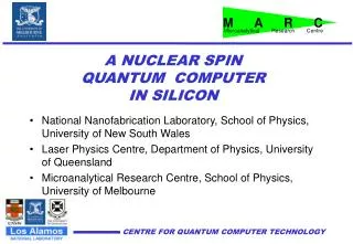
M A R C Microanalytical Research Centre A NUCLEAR SPINQUANTUM COMPUTERIN SILICON • National Nanofabrication Laboratory, School of Physics, University of New South Wales • Laser Physics Centre, Department of Physics, University of Queensland • Microanalytical Research Centre, School of Physics, University of Melbourne
Students Paul Otsuka MatthewNorman Elizabeth Trajkov Brett Johnson Amelia Liu* Leigh Morpheth David Hoxley* Andrew Bettiol Deborah Beckman Jacinta Den Besten Kristie Kerr Louie Kostidis Poo Fun Lai Jamie Laird Kin Kiong Lee Academic Staff David Jamieson Steven Prawer Lloyd Hollenberg Postdoctoral Fellows Jeff McCallum Paul Spizzirri Igor Adrienko +2 Infrastructure Alberto Cimmino Roland Szymanski William Belcher Eliecer Para Key Personnel • Geoff Leech* DeborahLouGreig • Ming Sheng Liu • Glenn Moloney • Julius Orwa • Arthur Sakalleiou • Russell Walker • Cameron Wellard*
The Quantum Computer: Melbourne Node Node Team Leader: Steven Prawer Test structures created by single ion implantation Atom Lithography and AFM measurement of test structures Theory of Coherence and Decoherence
Fabrication Pathways Fabrication strategies: • (1) Nano-scale lithography: • Atom-scale lithography using STM H-resist • MBE growth • EBL patterning of A, J-Gates • EBL patterning of SETs • (2) Direct 31P ion implantation • Spin measurement by SETs or magnetic resonance force microscopy • Major collaboration with Los Alamos National Laboratory, funded through US National Security Agency
30 keV e 60 keV e 2 MeV He 5 m 10 m 0.5 m • Deep probe • Large damage at end of range keV electrons and MeV ions interact with matter • Restricted to 10 m depth, large straggling • Low beam damage
The Melbourne Pelletron Accelerator • Installed in 1975 for nuclear physics experiments. • National Electrostatics Corp. 5U Pelletron. • Now full time for nuclear microprobe operation. • Will be state-of-the-art following RIEFP upgrade Inside Outside
x-ray detector 1 m From accelerator Scanner Beam steerer & Object collimators Aperture collimators Microscope Probe forming lens SSBs Sample stage goniometer Low vibration mounting Ion pumps Nuclear microprobe essential components
Re-entrant microscope port & light SSB detectors SiLi port Specimen Chamber inside • 30 mm2 Si(Li) x-ray detector • 25 and 100 msr PIPS particle detectors at 150o • 75 msr annular detector
MeV ions interact with matter 3 MeV H+ • MeV ions penetrate deeply without scattering except at end of range. • Energy loss is first by electronic stopping • Then nuclear interactions at end of range PMMA substrate(side view) surface 100 m
Micomachining Protons • Example • Proton beam lithography • PolyMethyl MethAcrylate (PMMA) • exposure followed by development • 2 MeV protons • clearly shows lateral straggling 10 m Sideview
The work of Frank Watt MeV ion beam micromachining:High aspect ratio structures in PMMA Work done at the Nuclear Microscopy Unit at the National University of Singapore • 2.3 MeV protons on PMMA • This work dates from 1996, much more interesting structures are now available • See review by Prof F. Watt, ICNMTA6 - Cape Town, October 1998
The work of Mark von Bibra 2 MeV H+ silica surface laser light emerging 20m MeV ion beam micromachining:Optical Materials • Fused Silica • Increase in density at end of range • Increase in refractive index (up to 2%) at end of range
The work of Mark von Bibra MeV ion beam micromachining:Layered Waveguides • Ion energy ---- waveguide depth
Single Ion Implantation Fabrication Strategy Etch latent damage& metallise Read-out state of “qubits” MeV 31P implant Resist layer Si substrate
Light ion etch pits Heavy ion etch pit Scale bars: 1 mm intervals MeV ion etch pits in track detector • Single MeV heavy ions are used to produce latent damage in plastic • Etching in NaOH develops this damage to produce pits • Light ions produce smaller pits 3. Etch 2. Latent damage 1. Irradiate From: B.E. Fischer, Nucl. Instr. Meth. B54 (1991) 401.
Single ion tracks • Latent damage from single-ion irradiation of a crystal (Bi2Sr2CaCuOx) • Beam: 230 MeV Au • Lighter ions produce narrower tracks! Depth 1 mm 3 mm 5 mm 7.5 mm 3 nm From Huang and Sasaki, “Influence of ion velocity on damage efficiency in the single ion target irradiation system” Au-Bi2Sr2CaCu2Ox Phys Rev B 59, p3862
High energy single-ion tracks in silicon: direct imaging with scanning probe microscopy • Nanofabrication by the implantation of MeV single-ions offers a novel method for the construction of small devices which we call atomic-lithography. A leading contender for the first nano-device constructed by this method is an array of spins for a quantum computer. For the first time, we propose the use of high resolution scanning probe microscopy (SPM) to directly image irradiation-induced machining along the ion track and lattice location of the implanted ion in silicon on an atomic scale. This will allow us to measure the spatial distribution of defects and donors along the tracks to analyse the atom-scale electronic properties of the irradiated materials. STM/AFM tip
Spin array test structure • Aim: Create a spin array for test imaging with MRAFM Grid <Si> Implant 31P through mask of 1 micron period grid 300 nm deep (220 keV 31P+) Resulting array of 1 micron islands of spins Number of spins in each island is 1x10⁻⁸D, D is 31P dose in P/cm2