Download
1 / 15
150 likes | 267 Views
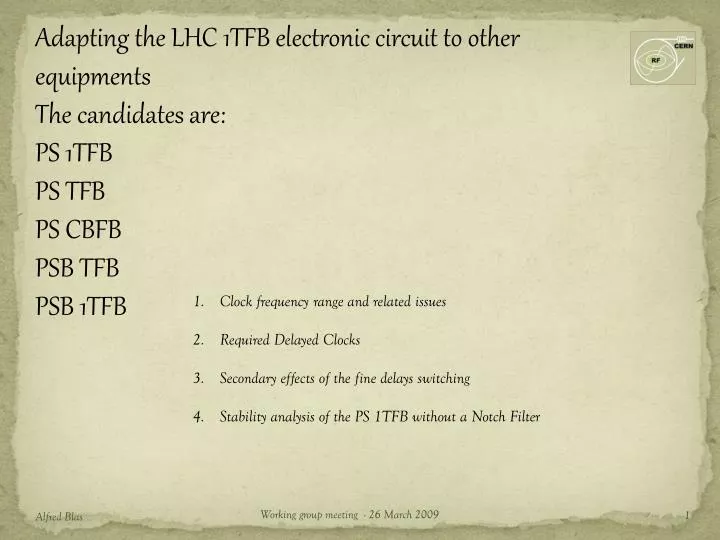
Adapting the LHC 1TFB electronic circuit to other equipments The candidates are: PS 1TFB PS TFB PS CBFB PSB TFB PSB 1TFB. Clock frequency range and related issues Required Delayed Clocks Secondary effects of the fine delays switching

E N D
Adapting the LHC 1TFB electronic circuit to other equipments The candidates are: PS 1TFB PS TFB PS CBFB PSB TFB PSB 1TFB Clock frequency range and related issues Required Delayed Clocks Secondary effects of the fine delays switching Stability analysis of the PS 1TFB without a Notch Filter Alfred Blas
Clock frequency range and related issues The most demanding equipment in that respect is the PSB TFB PSB revolution frequency with Linac2 [ 0.6 MHz , 1.73 MHz ] (factor 2.88) PSB revolution frequency with Linac4 [ 1 MHz , 1.73 MHz ] (factor 1.73) Sampling rate for having a 20 MHz system analogue bandwidth > 60 Ms/s Present ADC (AD6645) clock frequency range: [ 30 MHz , 105 MHz] DAC (AD9754) clock frequency range: [ DC , 125 MHz] Final limitation for the sampling frequency : 60 MHz < fS < 105 MHz The ratio 105/60 = 1.75 > 1.73 is compatible with a use in the PSB during the Linac4 era ! < 2.88 means it is not compatible with Linac 2! For a use within the Linac 2 era either: Change the ADCs / DACs Change the clock harmonic during the accelerating cycle Alfred Blas
Clock frequency range and related issues The most demanding equipment in that respect is the PSB TFB ADCs can be found with 16 bits and a clock frequency range = [ 30 MHz , 160 MHz ] Nevertheless there are at reasons not to change them: It requires resources that are lacking It would be only useful in the frame of Linac 2 which will be replaced in 2013 Keeping a high sampling rate by the mean of a clock harmonic change is much more efficient as it allows to keep a higher analogue bandwidth with the same hardware To be able to change the clock harmonic on the fly, the following conditions need to be fulfilled: Clock source and sampled device need to be synchronous for the change of harmonic The new harmonic value needs to be known (to allow the proper change of filters and delay parameters) The loop signal will not be available for the duration of the purging of the old data sampled with the previous clock harmonic ( 1 revolution). This shortcoming is not inevitable but is of little effect and allows a simplification of the hardware. Alfred Blas
Clock frequency range and related issues The most demanding equipment in that respect is the PSB TFB For the harmonic change to be synchronous on both the sending and receiving ends: The clock can be tagged… but the hardware would have to be modified at both ends A special trigger could be send in parallel with the clock signal (a: with a double twisted pair or b: with two coax cables of the same length). Prop. a means hardware and cabling changes; prop. b means to install new cables and doesn’t give precise results (although we could live with it (see below). The clock frequency could be measured online and when an abrupt change is detected the new harmonic is applied. For the new harmonic value to be known: The hclock values could be sent from the clock source as a serial word. This solution requires hardware changes and is heavy. The hclock values could be sent as the content of registers. The first register giving the value at injection and the others the following values. The central control system would update the registers on both ends on a ppm basis The hclock value could be measured online, but this is time consuming. The hclock values could be pre-determined once forever. Always the same value at injection; always the same clock frequency ratio at each change. This solution means no communication. Alfred Blas
Clock frequency range and related issues The most demanding equipment in that respect is the PSB TFB The proposed solution for the clock range issue is: Change the clock harmonic on the fly Have the sequence of harmonic values programmed in registers Detect the harmonic change in real-time from a measurement at the receiving end. The detector response time will mean that corrupted (wrongly sampled) data will be sent to the hardware; this is acceptable if this response time is smaller than a couple of clock periods Dump the invalid loop values acquired at the previous clock harmonic at the cost of no data for 1 turn Alfred Blas
Required delayed clocks The most demanding equipment in that respect is the PS TFB Data in Ck Write Address Counter DP RAM Ck Write Read Address Ck + calculated Δt Calculated pipeline delay Read 2 different clock domains ! Data out One delay needs to be applied to equalize the delay between 2 PUs; another needs to be applied to adapt the total loop delay. Alfred Blas
Required delayed clocks The most demanding equipment in that respect is the PS TFB When ΔT < tpd + th the read address needs to be latched with CK (tpd = CK to data out propagation delay, th = flip-flop hold time) When tpd + th < ΔT < TCK the read address needs to be latched with /CK (inverted CK) The diagrams on this page represent the situation with ΔT = 0 ns when the fine delay is programmed to zero (clock and delayed clock are in phase). This is not the case presently. Alfred Blas
Required delayed clocks The most demanding equipment in that respect is the PS TFB If ΔT was not equal to 0 ns when programmed to zero (actual case = 8.8 ns) the strategy would be more complicated and would require the knowledge of the offset delay. Value to be available in a data-base. => complicated handling. Alfred Blas
Required delayed clocks The most demanding equipment in that respect is the PS TFB To ease the operation of the board, he following setup is recommended: CK ΔToffset ΔToffset Rev clock CK + ΔT1 ΔTvar ΔToffset CK + ΔT1 + ΔT2 ΔTvar Alfred Blas
Required delayed clocks ADC Data synchronization ADC conversion time: 1.4 tC 7ns FPGA flip-flop hold time = 1ns? Longer path in the FPGA from pin to F-F compared pin to clock path :3ns? Alfred Blas
Required delayed clocks Data ADC 1 ADC CK ΔToffset ΔToffset ΔTADC /CK Rev clock CK + ΔT1 ΔT1 ΔToffset ΔTADC /(CK + ΔT1) Data ADC 2 ADC CK + ΔT1 + ΔT2 ΔT2 ΔTADC /(CK + ΔT1 + ΔT2) Alfred Blas
Effect of a delay change Data in Ck Write Address Counter DP RAM Ck Write Read Address Ck + calculated Δt Calculated pipeline delay Read Data out During an accelerating cycle the automatic delay will decrease in the following way: Smooth decrease of the fine delay Δt down to zero -> then decrease of one pipeline stage together with an abrupt increase of the fine delay Δt of about one clock period. Opposite behavior in a decelerating cycle. Alfred Blas
Effect of delay change This delay transition (decrease of one pipeline stage) should be smooth with no glitch. The memorized clock signal in the fine delay total length has no side effect (assuming a smooth functioning of the file delay chip). Alfred Blas
Analysis of 1TFB stability without the Notch Filter The analysis will be made with a gain compensation in the forward AVC loop path to compensate for the reduction due to the presence of a gain at the rf frequency in the feedback path. To be completed ! This analysis will have no consequences on the PCB architecture. Alfred Blas
Summary Things to be taken into account for the hardware development The ADCs should be kept as they are (although the 105 MHz version is preferred) The clock distribution should be implemented as described in slide 11. The smooth functioning of the fine delay chip should be checked for (no missing or extra clock rising edge when changing the delay value) The clock reception unit should be designed to deal with distant signals (ground decoupling) Alfred Blas