Download
1 / 16
160 likes | 183 Views
This detailed lecture recalls the different diode models, DC analysis, and representation in three models - ideal, piecewise linear, and diode AC equivalent. Explore the relationship between diode voltage and current components in AC analysis, along with circuit examples and calculations. Additionally, discover various types of diodes such as photodiode, solar cell, LED, and Schottky Barrier Diode, along with breakdown voltage and the Zener Effect. Dive into the operation of Zener diodes, circuit symbols, and the Avalanche Effect.

E N D
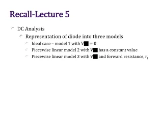
Recall-Lecture 5 • DC Analysis • Representation of diode into three models • Ideal case – model 1 with V = 0 • Piecewise linear model 2 with V has a constant value • Piecewise linear model 3 with V and forward resistance, rf
Sinusoidal Analysis The total input voltage vI = dcVPS + acvi iD= IDQ + id vD = VDQ+ vd IDQ and VDQ are the DC diode current and voltage respectively.
Total voltage Total current VDQ = DC voltage vd = ac component If vd << VT , the equation can be expanded into linear series as: The DC diode current IDQ in term of diode voltage VDQ
Therefore, the diode current-voltage relationship can be represented as The relationship between the AC components of the diode voltage and diode current is During AC analysis the diode is equivalent to a resistor, rd Where,
VDQ rd + - IDQ id DC equivalent AC equivalent
Example 1 Analyze the circuit (by determining VO & vo ). Assume circuit and diode parameters of VPS = 10 V, R = 5 kΩ, Vγ = 0.6 V & vi = 0.2 sin ωt DC Current DC Output voltage
vi vi
DC ANALYSIS AC ANALYSIS DIODE = MODEL 1 ,2 OR 3 DIODE = RESISTOR, rd CALCULATE rd CALCULATE DC CURRENT, ID CALCULATE AC CURRENT, id
EXAMPLE 1 • Assume the circuit and diode parameters for the circuit below are VPS = 10V, R = 20k, V = 0.7V, and vi = 0.2 sin t (V). Determine the current, IDQ and the time varying current, id ANSWERS IDQ = 0.465 mA id = 9.97 sin t (µA)
Other Types of Diodes The term ‘photo’ means light. Hence, a photodiode converts optical energy into electrical energy. The photon energy breaks covalent bond inside the crystal and generate electron and hole pairs Photodiode Solar cell converts visible light into electrical energy. The working principle is the same as photodiode but it is more towards PROVIDING the power supply for external uses Solar Cell
Light Emitting Diode An LED is opposite of photodiode this time, it converts electrical energy into light energy – Normally GaAs is used as the material for LED. During diffusion of carriers – some of them recombines and the recombination emits light waves. Schottky Barrier Diode A Schottky Barrier diode is a metal semiconductor junction diode. The metal side is the anode while the n-type is the cathode. But the turn on voltage for Schottky is normally smaller than normal pn junction diode
Breakdown Voltage • The breakdown voltage is a function of the doping concentrations in the n- and p-region of the pn junction. • Large doping concentrations result in smaller break-down voltage. • Reverse biased voltage – ET • The electric field may become large enough for the covalent bond to break, causing electron-hole pairs to be created. • So, electrons from p-type are swept to n-region by the electric field and holes from the n-type are swept to the p-region • The movement will create reverse biased current known as the Zener Effect.
Zener Effect and Zener Diode • The applied reverse biased voltage cannot increase without limit since at some point breakdown occurs causing current to increase rapidly. • The voltage at that point is known as the breakdown voltage, VZ • Diodes are fabricated with a specifically design breakdown voltage and are designed to operate in the breakdown region are called Zener diodes. Circuit symbol of the Zener diode: NOTE: When a Zener diode is reverse-biased, it acts at the breakdown region, when it is forward biased, it acts like a normal PN junction diode • Such a diode can be used as a constant-voltage reference in a circuit. • The large current that may exist at breakdown can cause heating effects and catastrophic failure of the diode due to the large power dissipated in the device. • Diodes can be operated in the breakdown region by limiting the current to a value within the capacities of the device.
e e e e atom atom atom h h h • Avalanche Effect • While these carriers crossing the space-charge region, they also gain enough kinetic energy. • Hence, during collision with other atoms, covalent bond is broken and more electron-holes pairs are created, and they contribute to the collision process as well. Refer to figure below Electron with high kinetic energy
Zener Diode 10 k Calculate the value of the current ID if VZ = 10V ANSWER: ID = 0.2 mA