Download
1 / 14
160 likes | 427 Views
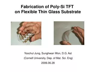
Fabrication of Poly-Si TFT on Flexible Thin Glass Substrate. Yoochul Jung, Sunghwan Won, D.G. Ast (Cornell University, Dep. of Mat. Sci. Eng) 2006.06.28. Outline. Motivation Comparison of Polymer and Glass substrates. Processing of Pocket Fabrication

E N D
Fabrication of Poly-Si TFT on Flexible Thin Glass Substrate Yoochul Jung, Sunghwan Won, D.G. Ast (Cornell University, Dep. of Mat. Sci. Eng) 2006.06.28
Outline • Motivation • Comparison of Polymer and Glass substrates. • Processing of Pocket Fabrication • 4. Characteristics of poly-Si TFT on Flexible Glass Substrate • 5. Summary and Discussion Ast Group
Motivation – Development of “Displays” TFT (poly-Si) -LCD TFT (a-Si) -LCD CRT Taken from Philips Inc. Advantages of flexible display Less apt to break, Roll-up, Less weight and volume Flexible Displays are being developed as the next generation displays Ast Group
Polymer substrates Glass substrates Polymer Based Display Vs. Glass Based Display Max. processing temperature ~ 300 °C Max. processing temperature ~ 600 °C Large CTE (PET, 65 x 10-6/°C) Low and adaptable CTE (Si, 2 x 10⁻⁶/°C) Mismatched with Si, thermal stress High surface finish Compatible material with xx surface finish to less compatible material α-Si:H α-Si:H Laser recrystallized Si with barrier layers CVD poly-Si Low temperature oxide MILC silicon Laser recrystallized Si (no thermal barrier) Ast Group
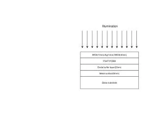
Source Gate Drain Gate Poly Si SiO2 Barrier layer (SiNx) Microsheet™ Glass Wafer Barrier layer (SiNx) SiO2 LPCVD Poly-Si TFT on MS Glass * Microsheet borosilicate glass contains boron * Boron acts as p-dopant in Si * Boron may migrate into Si-electronics during poly-deposition * Barrier layer is required1 * Mechanical support is required to handle Microsheet glass2 For 1, SiNX, LTO layer used for barrier layer For 2, Special support needs to be designed… Ast Group
Si-Framed Pocket Fabrication MS Glass substrate Real photo will be added here…. • No bonding between glass and Si piece rails • Free expansion and shrinkage • Controlling capillary phenomena Ast Group
Fabrication Process of Si-Framed Pocket 120 N, 350 °C, 1000 V Negative bias Pyrex Spacer (~ 500 m) Graphite chuck Bottom of EV 501 Bonder Chamber Si pieces (~ 300 m) Positive bias Si Si Bottom of EV 501 Bonder Chamber Positive bias Ast Group
Base line Characteristics (TFT on Si Wafer, Thermal Anneal) Vd(V) 10 5 0.1 Vg(V) 40 30 20 10 * W/L = 55um/8um * Poly-Si active layer: 620°C, 100nm * Gate oxide (LTO): 400°C, 100nm * Channel Mobility 7 cm2/Vs Ast Group
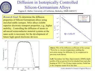
LPCVD poly-Si TFT on the Glass * TFT was short after thermal anneal * 580C poly-Si active layer * 620C, 24 hrs * SIMS data * Poly-Si active layer: 550°C, 100nm * Gate oxide (LTO): 400°C, 100nm Ast Group
Si Boron SIMS Analysis * After 620°C, 24 hrs anneal Boron diffused out from the glass ! * CTE mismatch caused thermal stress * Laser anneal was done instead of the conventional thermal anneal Ast Group
XRD of Poly-Silicon (Thermal, Laser Anneal) (111) (111) (220) 500C poly-Si on Glass 500C on Glass after Laser Anneal at 283 mJ Ast Group
Summary and Future Plan • 1. Fixture developed to process • 2. Base • 3. CVD poly • 4. Laser recrystallized • According to SIMS analysis, boron diffused into poly-Si layer after thermal annealing • of 620C, 24 hrs • * Future Plan * • Better effective Hydrogenation • Improvement of characteristics by Recrystallization • - Rapid Thermal Anneal (or standard anneal) • - Ni catalyzed crystallization • Stress and bending test • 4. Bending Ast Group
Acknowledgement CNF, a National Science Foundation supported National Nanofabrication Users Network (NNUN) Facility; Corning Inc.
![Thickness map [nm] of the poly-Si layer of a poly-Si/SiO 2 /Si multi-layer structure](https://cdn1.slideserve.com/2972061/slide1-dt.jpg)