
Exploring Vector-Register Architectures in Depth
E N D
Presentation Transcript
Appendix G Vector Processors in More Depth
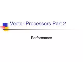
Figure G.1 Characteristics of several vector-register architectures. If the machine is a multiprocessor, the entries correspond to the characteristics of one processor. Several of the machines have different clock rates in the vector and scalar units; the clock rates shown are for the vector units. The Fujitsu machines’ vector registers are configurable: The size and count of the 8K 64-bit entries may be varied inversely to one another (e.g., on the VP200, from eight registers each 1K elements long to 256 registers each 32 elements long). The NEC machines have eight foreground vector registers connected to the arithmetic units plus 32 to 64 background vector registers connected between the memory system and the foreground vector registers. Add pipelines perform add and subtract. The multiply/divide-add unit on the Hitachi S810/820 performs an FP multiply or divide followed by an add or subtract (while the multiply-add unit performs a multiply followed by an add or subtract). Note that most processors use the vector FP multiply and divide units for vector integer multiply and divide, and several of the processors use the same units for FP scalar and FP vector operations. Each vector load-store unit represents the ability to do an independent, overlapped transfer to or from the vector registers. The number of lanes is the number of parallel pipelines in each of the functional units as described in Section G.4. For example, the NEC SX/5 can complete 16 multiplies per cycle in the multiply functional unit. Several machines can split a 64-bit lane into two 32-bit lanes to increase performance for applications that require only reduced precision. The Cray SV1 and Cray X1 can group four CPUs with two lanes each to act in unison as a single larger CPU with eight lanes, which Cray calls a Multi-Streaming Processor (MSP).
Figure G.3 Starting times and first- and last-result times for convoys 1 through 4. The vector length is n.
Figure G.4 Start-up penalties on VMIPS. These are the start-up penalties in clock cycles for VMIPS vector operations.
Figure G.5 The total execution time per element and the total overhead time per element versus the vector length for the example on page F-6. For short vectors, the total start-up time is more than one-half of the total time, while for long vectors it reduces to about one-third of the total time. The sudden jumps occur when the vector length crosses a multiple of 64, forcing another iteration of the strip-mining code and execution of a set of vector instructions. These operations increase Tn by Tloop + Tstart.
Figure G.6 Start-up latency and dead time for a single vector pipeline. Each element has a 5-cycle latency: 1 cycle to read the vector-register file, 3 cycles in execution, then 1 cycle to write the vector-register file. Elements from the same vector instruction can follow each other down the pipeline, but this machine inserts 4 cycles of dead time between two different vector instructions. The dead time can be eliminated with more complex control logic. (Reproduced with permission from Asanovic [1998].)
Figure G.7 Memory addresses (in bytes) by bank number and time slot at which access begins. Each memory bank latches the element address at the start of an access and is then busy for 6 clock cycles before returning a value to the CPU. Note that the CPU cannot keep all 8 banks busy all the time because it is limited to supplying one new address and receiving one data item each cycle.
Figure G.8 Timings for a sequence of dependent vector operations ADDV and MULV, both unchained and chained. The 6- and 7-clock-cycle delays are the latency of the adder and multiplier.
Figure G.9 Result of applying vectorizing compilers to the 100 FORTRAN test kernels. For each processor we indicate how many loops were completely vectorized, partially vectorized, and unvectorized. These loops were collected by Callahan, Dongarra, and Levine [1988]. Two different compilers for the Cray X-MP show the large dependence on compiler technology.
Figure G.10 The inner loop of the DAXPY code in chained convoys.