
연구 주제
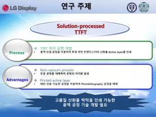
연구 주제. Solution-processed TTFT. TTFT 저가 공정 개발 용액 인쇄 공정을 이용하여 투명 박막 트랜지스터의 산화물 Active layer 를 인쇄. Process. Non-vacuum process 진공 공정을 대체하여 공정의 저가화 달성 Printed active layer 패턴 인쇄 가능한 공정을 이용하여 Photolithography 공정을 배제. Advantages. 고품질 산화물 박막을 인쇄 가능한 용액 공정 기술 개발 필요. 연구 방향 – active layer.

연구 주제
E N D
Presentation Transcript
연구 주제 Solution-processed TTFT • TTFT 저가 공정 개발 • 용액 인쇄 공정을 이용하여 투명 박막 트랜지스터의 산화물 Active layer를 인쇄 Process • Non-vacuum process • 진공 공정을 대체하여 공정의 저가화 달성 • Printed active layer • 패턴 인쇄 가능한 공정을 이용하여 Photolithography 공정을 배제 Advantages 고품질 산화물 박막을 인쇄 가능한 용액 공정 기술 개발 필요
연구 방향 – active layer • Active layer 물질 • ZnO, IGZO Materials • 인쇄 가능한 용액 공정 • 저온 공정 ( 300도 이하) • Device 성능 • Transmittance >90% • On/Off : >107 • Mobility: > 15 cm2/VS • Subthreshold slope < 1.5 V/decade Requirement Sol-gel Nano Particle • Sol-gel 방법을 이용한 접근 • 저온에서 조밀한 박막이 가능한 sol-gel precursor 물질 개발 및 공정 기술 개발 • 결정도 향상 공정 개발 • 나노입자를 이용한 접근 • 균일한 크기의 나노입자 합성 공정기술 개발- (sputter – ionic liquid) • 나노입자 잉크를 이용한인쇄 공정 개발 • 저온 나노 입자 소결 공정개발 (Field-assistedsintering 등…) Approach
연구 방향 – Dielectric layer • Approach • Additive High K material • Nano-particles (TiO2 , Al2O3, Y2O3) • TiO2 Precursor • TiO2 Synthesis • Goal • High on/off ratio • High dielectric constant Materialspolymer : PAA, PVP nano composite
연구 목표 • Transmittance >90% • On/Off : >107 • Mobility: > 15 cm2/VS • Subthreshold slope < 1.5 V/decade • Temp. < 300 degree FlexibleTransparent Transistor Patterning &printable process Compatibility Study Prototype TTFT Unit process Development 3차년도 2차년도 1차년도
TTFT Active layer transfer Reusable Substrate Oxide Semiconductor Channel Region Gate Dielectric Gate Electrode Substrate • High mobility • Large grain size at channel region • Robust process • No sputter damage on dielectric layer • Low leakage current Advantages