Download
1 / 33
330 likes | 351 Views
Detailed review of IBL sensor prototype programs, requirements, and recommendations from CERN meeting in May 2011.

E N D
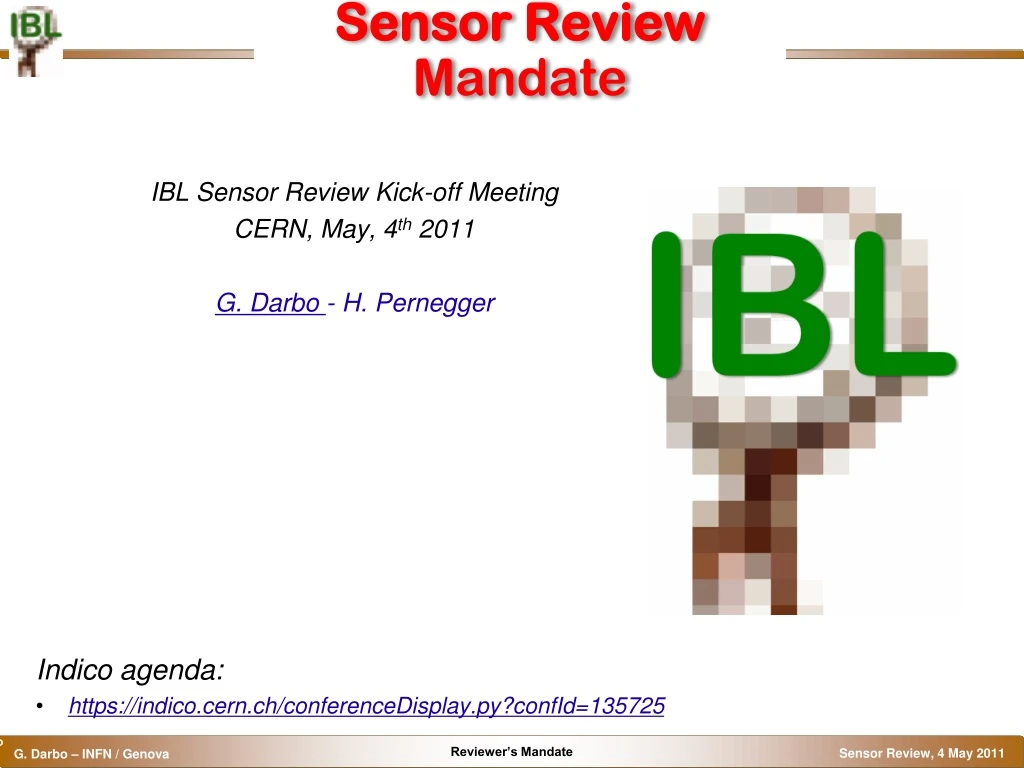
Sensor ReviewMandate IBL Sensor Review Kick-off Meeting CERN, May, 4th 2011 G. Darbo - H. Pernegger Indico agenda: https://indico.cern.ch/conferenceDisplay.py?confId=135725
Sensor Review Mandate - Outlook • Introduction • Module Prototype Program and Sensor R&D’s • Requirements for IBL • From IBL TDR • Quantities for production • Sensor designs for IBL: • Planar n-on-n and 3D design & floorplan • Sensor pre-production & production • Prototyping program & test (see Jörn’s talk) • Samples, Irradiation, Test Beam, Qualification Measurement • Status and plans for July • Reviewer's mandate • What is know, an what to look in depth
How to read the material Reviewer recommendation Introduction
Material for Review and Reviewer’s Mandate • Information is taken mostly from IBL TDR for specifications. • No information is given to measurements on FE-I4 devices with the reviewed sensors • Material will be collected in the next two months and prepared for the reviewers (we also expect feedback and request from reviewers). • Throughout the slides, It will be pointed out what is known and what still need to be done. • Review committee will be asked to evaluate: • Fulfilling the requirements • Look at performance, system issues, production readiness and schedule from foundries, yield and production quantities, risks and risk mitigation. • Give a weighted recommendation based on the information available at the review date. • The IBL Institute Board with the IBL Management plans to decide on one of the two sensor technologies based on the reviewers recommendations.
Module Prototype Program • Module prototype program in the IBL TDR (Summer 2010) consider for IBL: • Three sensor technologies, which addresses the IBL requirements with different trade-offs. • Planar sensor n-on-n and n-on-p, 3D sensors with active edge or slim edge, pCVD Diamond sensor • Extensive module prototyping, review in summer 2011, decision after review, pre-production and final production. • In January 2011 kick-off meeting to accelerate the IBL schedule for IBL installation in 2013/14 LHC shutdown (SD): • Two main motivations support the speed-up: • Machine has moved LHC next shutdown into 2013/14. phase I shutdown delayed (2017 or later) • Installation in 2013 simplified by low activation of beam pipe. • very good results from FE-I4 ask for minimum changes to final design • Support for speed up came from IBL Institutes and then from ATLAS. • “Sensor reaction” to speed-up: • Diamond consider that new schedule cannot fit with needed production time. • 3D and planar sensor discussed at large in IBL and in the ATLAS R&D collaborations. • Focus on two designs: • 3D double side with slim edge • Planar n-on-n with slim edge, • Prototyping of two design on speed lane and pre-production started Planar Sensors ATLAS Collaborations for HL-LHC R&D IBL 3D Sensors Diamond Sensors
The ATLAS 3D and PPS R&D Collaborations • ATLAS R&D activities for sLHC have been reviewed by the Upgrade Steering Group (USG) in the passed years. R&D’s programs, considered of interest of ATLAS, after internal review in the USG were approved by the ATLAS Executive Board. • ATLAS 3D Pixel Sensor R&D for sLHCproposal approved by ATLAS in 2007 • ATLAS Planar Pixel Sensor (PPS) R&D for sLHC approved by ATLAS in 2009 • The two R&D groups actively collaborate with IBL to provide sensors for IBL. • Activities in the past years focused on FE-I3 chip – several published papers from both collaborations • From last year FE-I4 sensor have been designed to be used with FE-I4 chip. • The two collaborations are independent from IBL, even if most of their members have “signed” the IBL TDR. • The sensor with FE-I4 layout, which are presently available, are part of R&D developments that have been coordinated between IBL and the ATLAS Pixel Sensor R&D’s. • ATLAS 3D Collaboration Institutes (Spokeperson: C.DaVià): Research Institutes: Bergen, Bonn, Cosenza, CERN, CTU Prague, Freiburg, Genova, Glasgow, Hawaii, IFAE Barcelona, LBNL, Manchester, New Mexico, Oslo, SLAC, Stony Brook, Trento, Udine Processing Facilities: CNM (Barcelona), FBK (Trento), SINTEF (Oslo)/Stanford, VTT (Finland) • ATLAS PPS Collaboration Institutes (Spokesperson: C.Gößling / Dortmund, Coordinator: D. Münstermann / CERN) Bonn, Berlin, CERN, DESY, Dortmund, MPP & HLL Munich, Udine, KEK, CNM Barcelona, Liverpool, LBNL, LPNHE, New Mexico, Orsay, Prague, Santa Cruz.
IBL Requirements: NIEL dose • Assumption in IBL TDR: • Total NIEL dose: 5 x 10¹⁵neq/cm2 • Comes from 550fb-1 integrated luminosity • Probably high from latest LHC forecast • With a safety factor of 60% • Simulated results are probably low: indication from measured data of higher value respect to simulation • Note: when samples are irradiated, should consider fluctuation and error in the in the actual exposed dose (the nominal value could have 10-20% uncertainties). • For the sensor review assemblies are irradiated and qualified at • NIEL = 5 x 10¹⁵neq/cm2 • TID = 250 Mrad Reference: TDR section 1.1.1
IBL Requirements: Efficiency • Hit efficiency in the active area of the sensors: • > 97% until after the total dose (ref: TDR table 7) • High pT tracks hit the sensors in IBL with a phi angle between 0º and 28º and an eta <2.58 (ref: TDR table 7) • Geometrical inefficiency: • < 2.6 % this requirement comes from TDR section 3.2 sensors: “The IBL module outline using 2-chip assemblies is shown in Fig. 41. In the case 3D sensors are chosen, the same outline can be produced using 1-chip assemblies with narrow sensor edges as shown in Fig. 42. Active edge technology to produce such narrow edges is a feature of 3D sensors. There is no shingling in z of the IBL modules due to the extreme radial space constraints, and this results in slightly difference geometric acceptance for 2-chip and 1-chip assemblies. For 1-chip (2-chip) assemblies the nominal acceptance for particles normal to the beam is 98.8% (97.4%).” • Comments: • Active edge 3D sensor have been dropped for the IBL speedup schedule. • Sensor isolation require insertion of a peek spacer between modules to isolate each other.
Requirements from Cooling • The target temperature for operating the IBL sensors is approximately -15 ◦C, in order to minimize effects of reverse annealing on the sensors and to avoid thermal runaway. • IBL design uses CO2 cooling fluid an Ti pipe. • Curves on right plot have been calculated for • Carbon Fiber pipe with Thermal Figure of merit [Kcm2/W] = 19 • Ti pipe with Thermal Figure of merit [Kcm2/W] = 4.5 • Some design changes on stave (smaller Ti pipe, face plate) require a more conservative Figure of merit value.
Hints to Tile Quantities for IBL ATLAS Pixel Module Yield Pixel modules has 16 FE chips – bump-bonding (BB) reworking (FE-I3 stripping and flipping a new one) Selection of Assembled module was done on ranking points (pt.). Accepted module: ranking <1000 B-layer module: ranking < 60 (0.13% dead pixels) Ranking includes: Bband WB reworking, bow, etc. One dead channel is 1 pt. Ref: G. Add et al., Atlas pixel detector electronics and sensors, Journal of Instrumentation, 3(07):P07007, 2008. Bare modules • For IBL modules is very different: • 1 or 2 chips instead of 16 → should be better for yield • But BB process is in development for thin and larger FE-I4 chip → yield largely unknown • Today is assumed that 2 times the sensor tiles that goes in the IBL (2x224 for double & 2x448 for single) is on the safety side . • It will be revised with acquired experience from built modules Dressed modules
CiS: Planar n-on-n CNM & FBK: 3D double side without active edge IBL SENSOR DESIGN
Planar Sensor – Slim Edge • IBL selected design for the Planar n-in-n technology has→ 200 μm slim edge • guard rings on p-side are shifted beneath the outermost pixels → least possible inactive edge • Less homogeneous electric field, but charge collection after irradiation dominated by region directly beneath the pixel implant → only moderate deterioration expected 200µm from pixel to dicing strip ~200÷250 µm inactive edge 500µm long pixels
Planar Sensors – “Conservative Design” • Not the IBL selected design, conservative design has: • Edge pixels of same length of core pixels • ~450 µm inactive edge • Several prototype assemblies with FE-I4 produced with conservative design edge. ~450µm inactive edge 250 µm pixels
CiS IBL Qualification Wafers • 6 FE-I4 sensors: • Conservative • slim edge • one 2-chip and two 1-chip sensors of each design • 12 FE-I3 SCs • various guard ring designs • diodes, test structures… • produced in 5 thicknesses: • Yield measured on 200µm thick wafer and 2-chip tiles is 83%.
Planar Sensors Pre-production Floorplan • IBL design: • 2 x FE-I4 chip modules; • n-on-n, 200µm thick, slim edge (~200µm); • Standard pixel size: 50x250µm • Column 1 & 160: 500µm wide • Column 80 & 81: 450µm wide • Wafer floorplan: • 4 IBL tiles • 4 single FE-I4 tiles, different designs • 4 single FE-I3 tiles, different design • Test structures Ref.: review indico document: Planar Pre-production wafer Description 2 x FE-I4 IBL DESIGN FE-I3 SC FE-I3 SC 2 x FE-I4 IBL DESIGN FE-I4 SC FE-I4 SC 2 x FE-I4 IBL DESIGN FE-I4 SC FE-I4 SC FE-I3 SC 2 x FE-I4 IBL DESIGN FE-I3 SC
3D Double Side Sensors • FBK and CMN have similar process • FBK full thru columns stopped by membrane. p-spray for pixel isolation • CNM stop etching before reaching opposite end. p-stop for pixel isolation • Same layout and column geometry in both designs • ~10µm column diameter • FBK full through, CNM column tip 15±7µm from opposite wafer surface. n+ etched and filled from top p+ etched and filled from bottom 700nm DRIE stopping membrane FBK DRIE: Full thru columns CNM DRIE: Almost full thru columns
3D Layout & Floorplan Common floorplan layout • Venice June 2009 • Full mechanical compatibility • Equivalence of performance • Compatible with single side (active edge) and double side Double side design • 200 µm ohmic fence (long stave direction). • 2 n+ columns per pixel (2E). Prototype / pre-prod. • Changed top metal and passivation masks to have bias voltage pad compatible with planar design. Cut line (80 µm) OHMIC FENCE TOP EDGE (200 µm) OHMIC FENCE LATERAL EDGE (400 /1500 µm) (right/left) n+ columns Pixel (50 x 250µm)
3D Sensor Pre-production Floorplan • IBL design: • 1 x FE-I4 chip modules; • 3D p-substrate, 2E structure,230µm thick, slim edge • (all) Pixel size: 50x250µm • Wafer floorplan: • 8 IBL tiles • 9single FE-I3 tiles • 3 CMS single FE tiles • Test structures • Prototype wafers: • Ref.: review indico document: • 3D Pre-production Wafer Description
Summary of CiS, CNM & FBK Batches • Note: FBK ATLAS07: • Batch used to tune the process (first full through column attempt) • Mask layout same as ATLAS 09 but some “weaknesses” in the process: • p-spray to low → low breakdown voltage • Contact resistance few order of magnitude to high → signal collection • Significant wafer bow due to border passivation → leakage current and yield • Accumulated experience → process modified for ATLAS09 • Note: single chip modules • Planar design consider 2-chip modules. The assemblies tested are all single chip equivalent, since the R/O system for 2-chip modules is in development Numbers and dates in Jörn’s talk
Sensor Pre-production • Not enough data available to make decision on sensors Planar: need more measurement with full radiation dose 3D: yield and production are the major unknowns Both: need adequate statistics on irradiated chip-sensor assemblies • To comply with the IBL speedup schedule: • Complete the prototype program while launching pre-production • Enough sensors (to start module production) will be ready of the selected technology when decision will be taken • Placed orders for 50 planar (CiS) and 50 3D sensors (FBK + CNM): • Planar selected slim edge design. Wafer thickness 200µm • 3D same wafer masks for both 3D producers: available form current prototypes. 230µm wafer thickness. • One additional batch started from each of the 3 producers. • Pre-production delivery: • CiS: 16-18 weeks, delivery 29/8/2011. • CNM: 36 weeks, delivery 30/10/2011. • FBK: 24 weeks, delivery 30/6/2011. CNM/FBK wafer mask 8 SC tiles/wafer CiS wafer mask 4DC tiles/wafer
Wafer Production QA/QC • CiS: • Tile selected by IV measurements using punch-through on wafer, re-measured after dicing. Similar to the ATLAS Pixel sensors. Test made at CiSbefore dicing. • CNM: • Measure the guard ring “fence” IV on wafer. • FBK: • Deposit removable metal to transform pixel to strips: 80 strips of 336 pixel. • Measure IV of individual strip – remove metal by etching • Specifications and QA/QC for all 3 wafer types in preparation • Some experience needed on prototypes to define criteria & cuts • Wafer to be produced: • CiS: with the measured yield (good statistics available) – 6 batches of 25 wafers satisfy IBL requirements • CNM+FBK: if yield is 50% are necessary 9/10 batches. If yield is 60% are necessary 8 batches.
What is on the safe side… • All three sensor producer have made sensors that unirradiated works • Tuning of the module is show be possible with low threshold (1500e or even lower). Systematic studies are going on. • No test beam analyzed results with FE-I4 assemblies of IBL design are available yet. From measurements made in the past years no big surprises expected. Critical for planar are the efficiency of long pixel and for 3D around the columns, specially at normal incidence • Charge provided by both sensor technologies is large enough to operate with a conservative discriminator threshold which gives low hit noise. • Planar design uses a consolidated technology, CiS was one of the two vendor that provided ATLAS Pixel sensor, from which the IBL design has been taken. Yield is expected to be well known. The two major differences between Pixel and IBL are: • Wafer thickness: 200µm in IBL instead of 250µm • Slim edge and Guard Ring (GR): GR reduced from 16 to 13 rings partially overlapping the edge pixels
What to look at… • After full dose: • Sensor operating conditions: IV, breakdown, leakage current, temperature dependence, stable operating threshold, noise, stability in time,… • Sensor performance: sensor efficiency in the active area, sensor efficiency inside the pixel (pixel edge, columns for 3D, punch-through for planar), noisy pixels per event after masking hot/dead pixels, charge sharing and cluster size at different angles,… • Process • Procedure to select good tiles on wafer. • Analysis of yield and good tiles. • Production schedule from foundries. • Additional issues • We expect additional requests from the reviewers on measurements or info • The IBL and sensor R&D communities will do their best to provide in the next 2 months.
Documents • Available on indico page: • IBL TDR, CERN-LHCC-2010-13, ATLAS TDR 19 • Planar talk at the AUW in Oxford • 3D talk at the AUW in Oxford • Planar pre-production wafer description • 3D pre-production wafer description • FE-I4 User’s manual • FE-I4 seminar • In preparation:
Contact Names • IBL Project Leader and Technical Coordinator • Giovanni Darbo / Genova, Heinz Pernegger/ CERN • ATLAS Planar Pixel Sensor (PPS) R&D: • Claus Gößling/ Dortmund (spokesperson), Daniel Münstermann/ CERN (coordinator), Reiner Klingenberg/ Dortmund (CiS production responsible) • 3D Sensor R&D spokesperson: • Cinzia Da Vià/ Manchester • Test beam and irradiation coordination: logistics, on-line and off-line analysis • Philippe Grenier/ SLAC, Alessandro La Rosa / CERN, Jens Weingarten / Göttingen • IBL Module WG coordinators • Maurice Garcia-Sciveres(FE-I4), Fabian Hügging/ Bonn (IZM bump-bonding) • Pixel and IBL software simulation coordinator: • Fares Djama/ Marseille CPPM