Communication Protocol for Writing to Configuration Register of TMP513 Device
This document outlines the communication process for writing to the configuration register of the TMP513 temperature sensor. It details the sequence of master and slave communications, including the acknowledgment process from the TMP513. The protocol includes using a 7-bit address for the TMP513, followed by a read/write (R/W) flag, data byte transmission, and clocking for data reading. The write operation involves both the Most Significant Bit (MSB) and Least Significant Bit (LSB). Proper understanding of this protocol is essential for successful data communication with the TMP513.

Communication Protocol for Writing to Configuration Register of TMP513 Device
E N D
Presentation Transcript
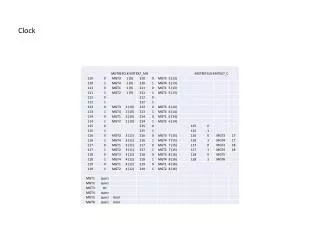
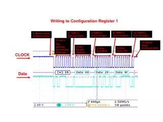
Writing to Configuration Register 1 8) TMP513 acknowledges 6) TMP513 acknowledges 10) TMP513 acknowledges 4) TMP513 acknowledges 1) Master Starts Communication 2) and 3) 7bit address followed by R/W Low 11) Master Stops Communication 5) 8bit Pointer Address 9) Data Byte LSB 7) Data Byte MSB CLOCK Data
Reading From Configuration Register 1 10) TMP513 acknowledges 4) TMP513 acknowledges 6) TMP513 acknowledges 1) Master Starts Communication 7) Master Starts Communication 12..Cont) Master Acknowledge 11..Cont) Master Acknowledge 2) And 3) 7bit address followed by R/W Low 8) And 9) 7bit address followed by R/W High 5) 8bit Pointer Address 11) Read MSB 12) Read LSB 13) Master Stops Communication CLOCK Data