Download
1 / 48
480 likes | 602 Views
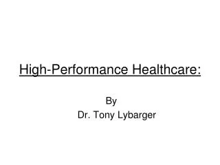
BG/L architecture and high performance QCD. P. Vranas IBM Watson Research Lab. :. BlueGene/L. A Three Dimensional Torus. System. 64 Racks, 64x32x32. BlueGene/L. Rack. Cabled 8x8x16. 32 Node Cards. 180/360 TF/s 32 TB. Node Card. (32 chips 4x4x2) 16 compute, 0-2 IO cards.

E N D
BG/L architecture and high performance QCD P. Vranas IBM Watson Research Lab P. Vranas, IBM Watson Research Lab
: BlueGene/L P. Vranas, IBM Watson Research Lab
A Three Dimensional Torus P. Vranas, IBM Watson Research Lab
System 64 Racks, 64x32x32 BlueGene/L Rack Cabled 8x8x16 32 Node Cards 180/360 TF/s 32 TB Node Card (32 chips 4x4x2) 16 compute, 0-2 IO cards 2.8/5.6 TF/s 512 GB Compute Card 2 chips, 1x2x1 90/180 GF/s 16 GB Chip 2 processors 5.6/11.2 GF/s 1.0 GB 2.8/5.6 GF/s 4 MB P. Vranas, IBM Watson Research Lab
BlueGene/L Compute ASIC P. Vranas, IBM Watson Research Lab
Dual Node Compute Card 206 mm (8.125”) wide, 54mm high (2.125”), 14 layers, single sided, ground referenced Heatsinks designed for 15W 9 x 512 Mb DRAM; 16B interface; no external termination Metral 4000 high speed differential connector (180 pins) P. Vranas, IBM Watson Research Lab
Midplane (450 pins) torus, tree, barrier, clock, Ethernet service port 32- way (4x4x2) node card 16 compute cards Ethernet-JTAG FPGA Custom dual voltage, dc-dc converters; I2C control 2 optional IO cards IO Gb Ethernet connectors through tailstock Latching and retention P. Vranas, IBM Watson Research Lab
360TF Peak; Footprint 8.5m x 17m; P. Vranas, IBM Watson Research Lab
64 racks at LLNL P. Vranas, IBM Watson Research Lab
BlueGene/L Compute Rack Power 87% ASIC 14.4W DRAM 5W per node 89% P. Vranas, IBM Watson Research Lab
BG/L is the fastest computer ever built . P. Vranas, IBM Watson Research Lab
BlueGene/L Link “Eye” Measurements at 1.6 Gb/s Signal path includes module, card wire (86 cm), and card edge connectors Signal path includes module, card wire (2 x 10 cm), cable connectors, and 8 m cable P. Vranas, IBM Watson Research Lab
Torus top level Processor Injection CPU Processor Reception CPU Net wires Net wires Net Receiver Net Sender P. Vranas, IBM Watson Research Lab
Torus network hardware packets The hardware packets come in sizes of S = 32, 64,… 256 Bytes P. Vranas, IBM Watson Research Lab
Torus interface fifos • The cpus access the torus via the memory mapped torus fifos. • Each fifo has 1Kbyte of SRAM memory. • There are 6 normal-priority injection fifos. • There are 2 high priority injection fifos. • Injection fifos are not associated with network directions. For example a packet going out the z+ direction can be injected into any fifo. • There are 2 groups of normal-priority reception fifos. Each group has 6 reception fifos, one for each direction (x+, x-, y+, y-, z+, z-). • The packet header has a bit that specifies into which group the packet should be received. A packet received from the z- direction with header group bit 0 will go to the z- fifo of group 0. • There are 2 groups of high-priority fifos. Each group has 1 fifo. All packets with the header high priority bit set will go to the corresponding fifo. • All fifos have status bits that can be read from specific hardware addresses. The status indicates how full a fifo is. P. Vranas, IBM Watson Research Lab
Torus communications code Injection • Prepare a complete packet in memory that has 8 bytes hardware header and the remaining bytes contain the desired payload. • Must be aligned at a 16 Byte boundary of memory (Quad aligned). • Must have size 32, 64, up to 256 bytes. • Pick a torus fifo to inject your packet. • Read the status bits of that fifo from the corresponding fifo-status hardware address. These include the available space in the fifo. • Keep polling until the fifo has enough space for your packet. • Use the double FPU (DFPU) QuadLoad to load the first Quad (16 Bytes) into a DFPU register. • Use the DFPU QuadStore to store the 16 Bytes into the desired torus fifo. Each fifo has a specific hardware address. • Repeat until all bytes are stored in fifo. • Done. The torus hardware will take care and deliver your packet to the destination node specified in the hardware header. P. Vranas, IBM Watson Research Lab
Torus communications code Reception • Read the status bits of the reception fifos. These indicate the number of bytes in each reception fifo. The status is updated only after a full packet is completely in the reception fifo. • Keep polling until a reception fifo has data to be read. • Use the double FPU (DFPU) QuadLoad to load the first Quad (16 Bytes) from the corresponding fifo hardware address into a DFPU register. • This is the packet header and has the size of the packet. • Use the DFPU QuadStore to store the 16 Bytes into the desired memory location. • Repeat until all bytes of that packet are read from the fifo and stored into memory. (you know how many times to read since the header had the packet size). • Remember that QuadStores store data in quad aligned memory addresses. • Done. The torus hardware has advanced the fifo to the next packet received (if any). P. Vranas, IBM Watson Research Lab
Routing Dynamic Virtual VC VC Cut-through VC VC with bubble escape VC VC and priority channel VCB VCP P. Vranas, IBM Watson Research Lab
Routing examples • Deterministic and adaptive routing • A hardware implementation of multicasting along a line P. Vranas, IBM Watson Research Lab
All to all performance 1,000 P. Vranas, IBM Watson Research Lab
The double FPU • The BG/L chip has two 440 cores. Each core has a double FPU. • The DFPU has two register files (primary and secondary). Each has 32, 64-bit floating point registers. • There are floating-point instructions that allow load/store and manipulation of all registers. • These instructions are an extension to the PowerPC Book E instruction set. • The DFPU is ideal for complex arithmetic. • The primary and secondary registers can be loaded independently or simultaneously. For example R4-primary and R4-secondary can be loaded with a single Quad-Load instruction. In this case the data must be coming from a Quad-aligned address. • Similarly with stores. P. Vranas, IBM Watson Research Lab
BlueGene/L and QCD at night : P. Vranas, IBM Watson Research Lab
Physics is what physicists do at night.R. Feynman P. Vranas, IBM Watson Research Lab
The 1 sustained-Teraflops landmark 1 sustained-Teraflops for 8.5 hours on 1024 nodes (1 rack) June 2004 P. Vranas, IBM Watson Research Lab
QCD on BlueGene/L machines (1/25/06) • More than 20 racks = 112 Teraflops worldwide mostly for QCD. • LLNL and Watson-IBM will possibly run some QCD. • … P. Vranas, IBM Watson Research Lab
MADD MADD MADD MADD One chip hardware External DDR 1GB For 2 nodes CPU0 L2 Pre-fetch L3 4 MB L1 32KB CPU1 L1 32KB 3D-Torus Fifos Tree Combine/Bcast Receiver Sender 5 ls roundtrip Virtual cut-through P. Vranas, IBM Watson Research Lab
QCD on the hardware 1) Virtual node mode: • CPU0, CPU1 act as independent “virtual nodes” • Each one does both computations and communications • The 4th direction is along the two CPUs (it can also be “spread” across the machine via “hand-coded” cut-through routing or MPI) • The two CPU’s communicate via common memory buffers • Computations and communications can not overlap. • Peak compute performance is then 5.6 GFlops CPU0 CPU1 P. Vranas, IBM Watson Research Lab
QCD on the hardware 2) Co-processor mode: • CPU0 does all the computations • CPU1 does most of the communications (MPI etc…) • The 4-th direction is internal to CPU0 or can be “spread” across the machine using “hand-coded” cut-through routing or MPI • Communications can overlap with computations • Peak compute performance is then 5.6/2 = 2.8 GFlops CPU0 CPU1 P. Vranas, IBM Watson Research Lab
Optimized Wilson D with even/odd preconditioning in virtual node mode • Inner most kernel code is in C/C++ inline assembly. • Algorithm is similar to the one used in CM2 and QCDSP: • Spin project in the 4 “backward” directions • Spin project in the 4 “forward” directions and multiply with gauge field • Communicate “backward” and “forward” spinors to nn • Multiply the “backward” spinors with gauge field and spin reconstruct • Spin reconstruct “forward” spinors P. Vranas, IBM Watson Research Lab
All computations use the double Hummer multiply/add instructions. • All floating computations are carefully arranged to avoid pipeline conflicts. • Memory storage ordering is chosen for minimal pointer arithmetic. • Quad Load/store are carefully arranged to take advantage of the cache hierarchy and the CPUs ability to issue up to 3 outstanding loads. • Computations almost fully overlap with load/stores. Local performance is bounded by memory access to L3. • A very thin and effective nearest-neighbor communication layer interacts directly with the torus network hardware to do the data transfers. • Global sums are done via a fast torus or tree routines. • Communications do not overlap with computations or memory access. • Small local size : Fast L1 memory access but more communications Large local size: Slower L3 memory access less communications. P. Vranas, IBM Watson Research Lab
Cycle breakdown For the Wilson Dslash operator with even/odd preconditioning. Processor cycle measurements (pcycles) in virtual node mode. The lattices are the local lattices on each core. P. Vranas, IBM Watson Research Lab
Wilson kernel node performance Spin-projection and even/odd preconditioning (“squashed” along x dir) Numbers are for single chip with self-wrapped links Full inverter (with torus global sum) P. Vranas, IBM Watson Research Lab
Weak Scaling (fixed local size) Spin-projection and even/odd preconditioning. Full inverter (with torus global sum) 16x4x4x4 local lattice. CG iterations = 21. P. Vranas, IBM Watson Research Lab
Special OS tricks (not necessarily dirty) • It was found that L1 evictions cause delays due to increased L3 traffic. In order to avoid some of this the “temporary” spin-projected two-component spinors are stored into memory with L1 attribute of write-through-swoa. • An OS function is called that returns a pointer to memory and a fixed size. That image of memory has the above attributes. This increased performance from 16% to 19%. • The on-chip, core-to-core communications are done with a local copy in common memory. It was found that the copy was faster if it was done via the common SRAM. • An OS function is called that returns a pointer to memory and a fixed size. That image of memory is in SRAM and has size about 1KB. This increased performance from 19% to 20%. • Under construction: An OS function that splits the L1 cache into two pieces (standard and transient). Loads in the transient L1 will not get evicted or cause evictions. Since the gauge fields are not modified during inversion this is an ideal place to store them. • These functions exist in the IBM Watson software group experimental kernel called controlX. They have not migrated to the BG/L standard software release. P. Vranas, IBM Watson Research Lab
Full QCD physics system • The physics code (besides the Wilson Dslash) is the Columbia C++ physics system (cps). • The full system ported very easily and worked immediately. • The BG/L additions/modifications to the system have been kept isolated. Acknowledgement We would like to thank the QCDOC collaboration for useful discussions and for providing us with the Columbia physics system software. P. Vranas, IBM Watson Research Lab
: BlueGene next generations P. Vranas, IBM Watson Research Lab
P P. Vranas, IBM Watson Research Lab
Q P. Vranas, IBM Watson Research Lab
? What would you do P. Vranas, IBM Watson Research Lab
… if they come to you with 1 Petaflop for a month? P. Vranas, IBM Watson Research Lab
: QCD, the movie P. Vranas, IBM Watson Research Lab
QCD thermal phase transition a clip from a BG/L lattice simulation. This clip is from a state of the art simulation of QCD on a ½ a rack of a BG/L machine (2.8 Teraflops). It took about about 2 days. It shows 2-flavor dynamical QCD on a 16x16x16x4 lattice with the DWF 5th dimension set to 24 sites. The pion mass is about 400 MeV. The color of each lattice point is the value of the Polyakov loop which can fluctuate between -3 and 3. Think of it as a spin system. The graph shows the volume average of the Polyakov line. This value is directly related to the single quark free energy. In the confined phase there are no free quarks and the value is low (not zero because of screening), in the quark-gluon plasma phase quarks can exist alone and the value is large. G. Bhanot, D. Chen, A. Gara, P. Heidelberger, J. Sexton, P. Vranas, B. Walkup P. Vranas, IBM Watson Research Lab