Download
1 / 52
520 likes | 669 Views
EECS 470. Busses in the real world Lecture 22 – Fall 2013. Today’s lecture. I want to talk about interconnects. There are tons of them on a computer Some to memory Some to I/O There have been lots of implementations I’m going to talk mostly about two older ones: PCI and P6

E N D
EECS 470 Busses in the real world Lecture 22– Fall 2013
Today’s lecture • I want to talk about interconnects. • There are tons of them on a computer • Some to memory • Some to I/O • There have been lots of implementations • I’m going to talk mostly about two older ones: • PCI and P6 • But I’m also going to talk a bit about newer ones • Quick Path and (very little) PCI Express • Let’s first look at the big picture.
Basic bus issues • What are the basic wires for specifying the transaction and moving the data • What are the types of transactions? How are they specified? • How is length of data transfer specified? • Who can delay (insert wait states?) • How is arbitration done? • Out-of-order transfers allowed? • Any restrictions? • Error reporting? • Weirdness? • Alignment for example.
Transaction types • Usually read/write with a length • But in a given domain, other info might be important. • Data vs. Code access. • I/O vs. memory access • Hints to target device • Length might be arbitrary.
Delaying • Who can delay and how • Usually a target (slave) can delay • Sometimes initiator (master) can delay • Sometimes initiator can drop the transaction • Sometimes the target has options on how to delay.
Arbitration • Fairness • Even sharing, priority sharing, weighted sharing • Mechanism • Centralized arbiter • Distributed arbiter • Combination • Duration • Until done • Until someone else requests • Until certain time passes. • Combination
Out-of-order • Does the bus allow transactions to complete out-of-order? • If so, can increase bandwidth (why?) • If so, might have to worry about ordering issues • Memory consistency models not a topic for this class (take EECS 570!) but basics are pretty easy to grasp
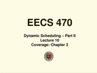
BSB BSB L2 L2 Proc Proc P6 bus Chipset Mem PCI PCI • PCI stands for “Peripheral Component Interconnect • Many cards you plug into a computer are PCI (most network cards, older graphics cards, etc.) • Normal configurations have PCI as a 33MHz bus with a 32 bit shared address/data lines. • This is based on version 2.1 of the PCI spec. • Changes with 3.0 and 2.3 are fairly minor from our viewpoint.
Speeds • Conventional PCI is at version 2.3 • Basic version is 32-bits at 33MHz and 5 volts • Version 2.1 allowed 5V or 3.3V and up to 64bit 66MHz • PCI-X • Backwards compatible (but not 5 volts apparently) • Up to 533MHz with only 1 load
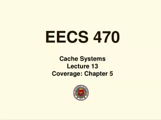
AD[31:0] Address/data and command C/BE#[3:0] PCI Master Device (required signals only) PAR REQ# Arbitration FRAME# GNT# TRDY# CLK Interface control System IRDY# RST# STOP# PERR# Error reporting DEVSEL# SERR#
Basics • AD[31:0] bus is for the address and the data • The C/BE#[3:0] is the Command in the address phase and the Byte Enablein the data phase • FRAME#, TRDY#, IRDY# are main control signals. • Other signals: • PAR is even parity over AD and C/BE# buses. • PERR# and SERR# are Parity and System error reporting • CLK is clock • RST# is a request to reset all devices.
AD and C/BE • AD • First phase is address • Everything afterwards is data • C/BE# • First phase is command • Rest is byte enable.
Control • FRAME# is asserted during the first phase of the transaction and until the last data phase. • TRDY# indicates that the target has valid data on the bus (READ) or is able to read valid data (WRITE) • IRDY# is the same as TRDY# but for the initiator.
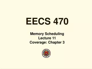
CLK AD[0:31] ?? ADS D1 D2 D3 FRAME# C/BE# ?? CMD BE BE BE IRDY# TRDY# Simple PCI read transaction
Simple PCI read transaction cont. CLK AD[0:31] ?? ADS D1 D2 D2 D3 FRAME# C/BE# ?? CMD BE BE BE IRDY# TRDY#
Deep thoughts with Mark • Notice that the length of the transaction is not specified explicitly • Starts at the given address. Keeps giving next data until done. • But this makes things hard for the target. How much data should be fetched? • So the various read commands give hints about how much data to move • Read is for less than a cache line • Read line is for a cache line or so • Read multiple is for more than 1 or 2 cache lines
More deep thoughts • It turns out many NIC cards did things in a really wacky way. • They would read (and/or write) 4KB pages by reading 4 bytes, going away, reading 4 more bytes • This caused significant problems on high-end (web) server performance. • But was okay on most workstations/desktops. • Moral: There is a cost vs. performance trade-off on almost everything you do. Be sure to consider the ramifications of solving the problem for only one domain.
Try to draw the write… CLK AD[0:31] FRAME# C/BE# IRDY# TRDY#
CLK AD[0:31] ?? ADS D1 D2 D3 D4 FRAME# C/BE# ?? CMD BE BE BE BE IRDY# TRDY# One solution
PCI write types • Memory Write • Just says gonna write • Memory Write and Invalidate • Writing • Will (100% promise!) that will start and end on cache line boundaries. • Why is this useful?
PCI Arbitration • Hidden phase • That is, done in parallel with transfers • Centralized arbiter • Arbitration algorithm unspecified, but must be “fair” • Fair isn’t all that fair… • #REQ, #GNT • Get bus when #GNT asserted, and FRAME, TRDY#, IRDY# not asserted. • Must give up when #GNT de-asserted in some reasonable time. • Notice, arbiter has separate grant and request lines for each PCI master…
Ordering • PCI target can say “go away” • STOP# signal • Initiator is obligated to come back to finish request. • (Notice with #FRAME the target can tell if transaction was done anyways) • Any ordering restrictions not PCI problem.
Basic bus issues: PCI? • What are the basic wires for specifying the transaction and moving the data • What are the types of transactions? How are they specified? • How is length of data transfer specified? • Who can delay (insert wait states?) • How is arbitration done? • Out-of-order transfers allowed? • Any restrictions? • Error reporting? • Weirdness? • Alignment for example.
BSB BSB L2 L2 Proc Proc P6 bus Chipset Mem PCI Basics of the P6 bus • The goal of the P6 bus is to allow communication among the processors and the chipset • Transactions are directed toward the chipset. • All of the processors “snoop” the bus. • It uses about 170 pins total
Basics of the P6 bus (cont.) • There are generally 6 phases of a transaction. • Arbitration - ask to use the bus • Request - Send Transaction details (R/W, size) • Error - parity error on request mainly • Snoop - let other processors get involved • Response - The “Ack” • Data transfer - Actual movement of data • In general the same phase of two transactions are separated by 3 clocks.
Why bother? • The goal of this part of the presentation is to expose you to a more complex bus. • The bus is a true “split-transaction” bus • That is, it is pipelined. • Increased bandwidth due to overlapping of accesses • No real impact on latency (why?) • It is the most complex bus I’m aware of. • Newer versions of the bus (P3, P4, Itanium) have some changes, but basics are the same.
Bus protocol • Each device on the bus has to be fairly sophisticated. • Arbitration is handled without a centralized arbiter. • Each device must keep track of the order of the transactions and which transaction is in what stage. • This ordering is called the “In order queue” or IOQ. • In addition there are “Out of Order” transactions. • These are used for transactions which are likely to take a while. (So they don’t interfere with the others)
1 2 3 4 5 6 7 8 9 10 11 12 13 14 15 16 CLK ARB 1 2 REQ 1 1 2 2 ERROR 1 2 SNOOP 1 2 RESP 1 2 DATA 1 2 One or more clock ticks Timing between phases
Phase 1: Arbitration • The arbitration phase mainly involves 5 pins • BREQ#[0:3] - Symmetric agent request • BPRI# - Priority agent request • Each processor keeps track of a rotating ID • The rotating ID is the last device to perform a bus transaction • Each device is only allowed to perform one transaction at a time if other devices also want to use the bus • If more than one device wants to use the bus the winner is the device which is “next” • So if the current ID is 2 the priorities are 3, 0, 1, 2 • If it is 0 the order is 1,2,3,0.
The arbitration rules • The device must continue to hold BREQ asserted until the clock before it gets asserts ADS# (starts the transaction) • Once a device starts its transaction it must deassert its BREQ line if any other BREQ line is asserted. • On the clock it’s BREQ is deasserted all devices re-compute which device will be allowed to go next. • Each agent updates its rotating ID after it deasserts BREQ# • If the bus is idle then it can assert ADS# two clocks after winning arbitration. • Each ADS# assertion must be at least 3 cycles apart.
Symmetric Arbitration example(with bus parking…) 1 2 3 4 5 6 7 8 9 10 11 12 13 14 15 16 CLK BREQ0 BREQ1 BREQ2 BREQ3 0a 1a 2a 0b 0c ADS# R. ID 3 3 3 3 0 0 1 1 1 2 2 2 0 0 0 0 Active? N N Y Y Y Y Y Y Y Y Y Y Y Y Y Y
0 has a request at time 2 and 91 has a request at time 12 has a request at time 7 1 2 3 4 5 6 7 8 9 10 11 12 13 14 15 16 CLK BREQ0 BREQ1 BREQ2 BREQ3 ADS# 3 3 R. ID N N Active?
Request • There are about 40 pins involved in this phase • The phase lasts 2 clocks. • The total of 80 signals (2 x 40) includes: • 36 bit address • Type of transaction • Byte enables • Size of transaction • Code/Data info • The #ADS signal “qualifies” the request signals • It is low during the first clock of the request phase.
Error • Fairly trivial. • Parity is checked for. • If the Parity check fails then AERR# is asserted. • All transactions in the IOQ are canceled and everything starts over. • I believe current implementations may crash with a parity error at this point.
Snoop • There are only 3 signals in the snoop phase • HIT#, HITM#, and DEFER# • None-the-less the snoop phase is the most complex part of the whole P6 protocol. • HIT# • If a processor has the data in its cache in the Shared or Exclusive state it asserts HIT# • HITM# • Is asserted by a processor if it has a “dirty” or Modified version of the data in its cache
Snoop (cont.) • DEFER# • Is only asserted by the chipset (or perhaps by some other priority agent). • It says that the chipset wants to pull this transaction out of the IOQ because it could take a while to respond. • DEFER# can also result in a “retry” request • If HIT# and HITM# are asserted • It is a snoop stall (ie. an agent on the bus could not respond to the request in time) • Snoop results are re-checked in 2 clocks
Snoop (cont.) • If HITM# and DEFER# are asserted • The DEFER# is ignored. • If HITM# is asserted • The processor asserting HITM# is responsible for supplying the data • The chipset is expected to “snarf” the data (ie. copy it into the DRAM) as it passes by. • Once the snoop phase has happened and DEFER# has not been asserted the transaction must complete.
Response Phase • This phase is mostly concerned with 3 signals, called RS[0:2]. • The 8 different orderings of these signals encodes the following possibilities: • Hard Failure -- Something went VERY wrong • Implicit Writeback -- HITM# was asserted • Deferred -- Transaction deferred • Retry -- Only if DEFER# was asserted • Normal Data -- Standard response • No Data -- Transaction requires no data
Data Phase • This phase consists of • 64 bits of data D[0:63]# • A DRDY and TRDY (pretty much the same as IRDY and TRDY on PCI) • All transactions are one of: • 0 bytes -- Invalidate • 8 bytes or less -- Write thru mode and uncacheable addresses will do this • 32 bytes -- moving a whole cache line • Which one it will be was determined during the request and snoop phases • What does the snoop phase have to do with it?
1 2 3 4 5 6 7 8 9 10 11 12 13 14 15 16 CLK ARB 1 2 REQ 1 1 2 2 ERROR 1 2 SNOOP 1 2 RESP 1 2 DATA 1 2 One or more clock ticks P6 Review
L2 Cache L2 Cache Processor Processor Memory & I/O Chipset Front Side Bus (Processor bus) Memory I/O I/O I/O I/O PCI bus (I/O bus)
QuickPath Interconnect • Here things are all point-to-point. • No shared bus • Can be as simple as a single processor talking to the chipset • Can be as complex as picture shown. • Memory and I/O interfaces are different Largely taken from: https://en.wikipedia.org/wiki/Intel_QuickPath_Interconnectand http://www.intel.ie/content/dam/doc/white-paper/quick-path-interconnect-introduction-paper.pdf
Details • QPI has two 20-bit signals, one in each direction • Each direction also has a clock • So 42 signals. • Each signal is a differential pair • Thus 84 pins. • 80-bit “flit” is the packet size. • Transferred in two clock cycles (four 20 bit transfers, two per clock.) • The 80-bit "flit" has 8 bits for error detection, 8 bits for "link-layer header," and 64 bits for "data". • Thus 8 bytes of useable information per 2 clocks in both directions.
Higher-level protocols • These 64-bit packets can be used for anything • Addresses • Data • Routing information • etc. • Wires no longer are the thing (address, data, etc.) • More complex for hardware, but so what?
Point-to-point?What about snooping • We’re back to a network. • So we need a directory-based solution. • Uses a variation of MESI, MESIF • F state is like shared, but is allowed to supply clean data • Why? • Has two schemes for doing snooping. • Home snoop • Source snoop