Download
1 / 73
730 likes | 853 Views
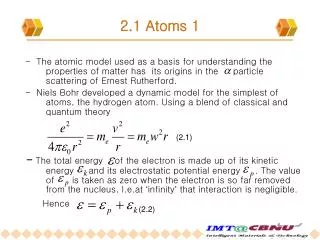
2.1 Atoms 1. - The atomic model used as a basis for understanding the properties of matter has its origins in the particle scattering of Ernest Rutherford.

E N D
2.1 Atoms 1 - The atomic model used as a basis for understanding the properties of matter has its origins in the particle scattering of Ernest Rutherford. - Niels Bohr developed a dynamic model for the simplest of atoms, the hydrogen atom. Using a blend of classical and quantum theory - The total energy of the electron is made up of its kinetic energy and its electrostatic potential energy . The value of is taken as zero when the electron is so far removed from the nucleus, I.e.at ‘infinity’ that interaction is negligible. Hence (2.1) (2.2)
2.1 Atoms 2 Substituting from equation (2.1) gives ※ From the quantum condition for angular momentum, which, substitutes with equation (2.1),leads to or (2.3) (2.4) (2.5)
2.1 Atoms 3 which substitutes into equation (2.3) to give ‘de Broglie wavelength’ Electron states are described by the solutions of the following equation which was developed by Erwn Schrodinger and which bears his name: (2.6) (2.7) (2.8)
2.1 Atoms 4 This from of the Schrodinger equation is independent of time and so is applicable to steady state situation, The symbol denotes the operator To apply equation (2.8) to the hydrogen atom it is first transformed into polar coordinates and then solved by the method of separation of the variables, This involves writing the solution in the form (2.9)
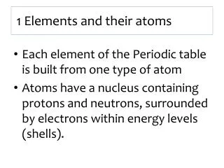
2.1 Atoms 5 - Pauli Exclusion Principle states that there cannot be more than one electron in a given state defined by particular set of values for and . For a given principal quantum number there are a total of available electronic. -Electrons occupy states such that following. 1.The value is maximum allowed by the Pauli Exclusion Principle,I.e. the number of unpaired spins is a maximum. 2. The value is the maximum allowed consistent with rule 1. 3. The value of when the shell is less than half-full and when it is mire than half-full. When the shell is just half-full, the first rule requires so that .
-page 9 • -page 10~11 with reference
2.2 The arrangement of ions in ceramics • Fig 2.1(a) in simple cubic packing, the centres of the ions lie at the corners of cubes formed by eight ions. it is generally found that anion lattices will accommodate oversize cations more readly than undersize cations so that the tolerance to the relatively small ion is exceptional • Fig 2.1(b) and (b)The oxygen ions are more closely packed together in the close-packed hexagonal and cubic structures. Fig 2.1 Packing of ions (a)simple cubic packing showing an interstice with eightfold coordination ; (b)hexagonal close packing; (c)cubic close packing showing a face-centred cubic cell
2.2 The arrangement of ions in ceramics • Fig 2.2(a) on this basis the rutile from of consists of columns of edge-sharing octahedra linked by shared coners of the units • Fig2.2(b)A hexagonal from of ,where the lattice is hexagonal close packed,contains layers of corner-sharing groups(Fig2.2(c)) Fig 2.2 octahedra arrangements in (a)perovskite-type structures, (b) And (c)hexagonal
2.3 Spontaneous polarization • Value of a crystal property depend in the direction of measurement • Crystals having cubic symmetry are optically isotropic • For these reasons, a description of the physical behaviour of a material has to be based ion a knowledge of crystal structure • Purpose to distinguish polar crystals, spontaneously polarized and possess a unique polar axis, from the non-polar variety • Of the 32 crystal classes, 11(centrosymmetric) and non-polar variety • Of the remaining 21 non- centrosymmetric classes, 20(piezoelctric, of these 10 are polar) • An idea of the distinction between polar and non-polar structures can be gained from Fig.2.3 Fig.2.3 (a) Non-polar array; (b),(c) polar arrays. The arrows indicate the direction of spontaneous polarization Ps
2.3 Spontaneous polarization • Piezoelectric crystals : when stressed, polarized or change in polarization When an electric field is applied, become strained • The 10- polar crystal types(pyroelectric, piezoelectric) : because of their spontaneous polarization • Pyroelectric crystal :change in temperature => change in spontaneous polarization additional features cannot be predicted from crystal structuresome material that the direction of the spontaneous polarization can be changed by an applied electric field or mechanical stresschange due to electric field = said to ‘ferroelectric’change due to stress = said to ‘ferroelastic’ • Poling process: conditions of temperature and time, static electric field after poling => ferroelectric ceramic makess it capable of poezoelectric, pyroelectric, electro-optical behaviour
2.3 Spontaneous polarization • The changes in direction of the spontaneous polarization: -The tetragonal(4mm) structure allows six direction-The rhombohedral(3m) allows eight direction-both tetragonal and rhombohedral crystallites are present at a transition point, the number of alternative crystallographic directions rises to 14 and the extra alignment attained becomes of practical significance
2.4 Transitions -Ionic size and the forces are both temperature dependent and may change sufficiently for a particular structure to become unstable and to transform to a new one -If a system is described in terms of the Gibbs function G then, because the molar entropies and molar volumes of the two phase do mot change, the change in G for the system can be written dG =- SdT + Vdp -It follows that -‘first-order’ transition: if there is a discontinuity in the derivative of G(T) there is a change in entropy at constant temperature, which implies latent heat -‘second-order’ transition: when the first derivative of the Gibbs function is continuous but the second derivative is discontinuous S : entropy , V : volume , P: pressure G G Latent heat T T T T Free-energy changes at transitions : (a)fist-order transition; (b) change in S at constant T and, consequently, latent heat; (c)second-order transition; (d)continuous change in entropy and so no latent heat (discontinuity in )
2.5 Deffects in crystals1 2.5.1 Non-stoichiometry -Manganese dioxide is a well-established compound but it always contains less than the stoichiometric amount of oxygen :The positive charge deficiency can be balanced by vacant oxygen site -Iron monoxide always contains an excess of oxygen :The charge excess can be balanced -LiNbO3 :The O ions are hexagonally close packed with a third of the octahedral sites occupied by Nb ,a, third by Li and a third empty. :This can be deficient in lithium down to the level Li0.94Nb1.012O3. :There is no corresponding creation of oxygen vacancies.instead the Nb content increases sufficiently to preserve neutrality -BaTiO3 :there is marked difference in charge and size between the two cations corresponding to differences between their lattice sites,to complete solid solutions over the whole possible range where the ions are identical in charge and close in size and can only occupy one type of available lattice site such as, Zr and Ti in Pb(ZrxTi1-x)O3 5+ + 5+ 4+
2.5 Deffects in crystals2 2.5.2 Point defects
2.5 Deffects in crystals3 -Point defects :They occur where atoms are missing(vacancies) or occupy the interstices between normal sites(interstitials):’foreign’ atom are also point defects -Line defects,or dislocations :They are spatially extensive and involve disturbance of the periodicity of the lattice -Frenkel and Schottky Defects: paired anions and cations • Electronic neutrality must be maintained in crystal. • Defects must come in pairs to maintain Q=0. • Cation-vacancy + Cation-interstitial = Frenkel Defect (Q=0) • In AX-type crystals, • Cation-vacancy + Anion-vacancy = Schottky Defect (Q=0)
2.5 Deffects in crystals4 -The equilibrium concentrations of defects in a simple binary oxide MO -The notation of Kroger and Vink -In summary,a chemical equation involving defects must balance in 3 respects 1.the total charge must be zero; 2.there must be equal numbers of each chemical species on both sides; 3.the available lattice sites must be filled,if necessary by the introduction of vacant sites nS&nF: Schottky and Frenkel defect concentrations respectively ΔHS&ΔHF:enthalpy change accompanying the formation of the associated defects. (cation vacancy+ anion vacancy and ion vacancy + interstitial ion) N :concentration of anions or cations N`:concentration of available interstitial sites . Net positive, negative .. . interstitial vacancy
2.5 Deffects in crystals5 4+ 3+ .. (2.15) -The introduction of an acceptor Mn on a Ti site in BaTiO3 can be expressed as ⇌ -which replaces the equilibrium equation for the pure crystal ⇌ -Since BaO=BaBa+Oo, equation(2.15) simplifies to ⇌ -The equilibrium constant for equation(2.16) is -KA is expressed as a function of temperature by -The replacement of Ba in BaTiO3 by the donor La is represented by ⇌ -The equilibrium constant KD is .. (2.16) .. ΔHA : change in enthalpy of the reaction K`A : temperature-insensitive constant 3+ . n: electron concentration
2.6 Electrical conductuion1 2.6.1 Charge transport parameters -The current density j will be given by j=nQv -If the drift velocity of the charge is proportional to the force acting on them, v=uE j=nQuE -For materials for which nQu is constant at constant temperature Ohm’law: u : mobility :σ(conductivity) = nQu =(1/ρ) v v Q A E Flow of charge in a prism
2.6 Electrical conductuion2 8 Metals Semi-conductors and semi-insulators 4 -The room temperature values of conductivity characteristic of the broad categories of material 0 -4 insulators -8 -12 -16 T/K 300 1000 Conductivities of the various classes of material:shading indicates the range of values at room temperature Conductivity characteristics of the various classes of material
2.6 Electrical conductuion3 2.6.2 Electronic conduction • Band conduction Empty conduction band Partly filled band Forbidden zone EF Valence band Bands arising from inner electron levels Energy (a)Atomic levels having identical energies merging to a broad band of levels differing slightly in energy as free atoms condense to form a crystal; (b) band structure At equilibrium interatomic spacing in a crystal. Schematic electron energy band structures for (a) a metallic crystal and (b) a semiconducting or insulating crystal
2.6 Electrical conductuion4 -The electron density in the conduction -The Fermi-Dirac function F(E) Z(E)dE: total number of states in the energy range dE around E per unit volume of the solid (2.28) EF : Fermi energy (2.29) Conduction band - - - - - - - - - - - - - - Ec Energy Eg EF Ev + + + + + + + + + + + + + + Valence band Band structure with electrons promoted from the valence to the conduction band
2.6 Electrical conductuion5 - E-EF>>kT : at room temperature kT≒0.025eV , E-EF: over the 0.2eV the term +1 can be omitted from equation(2.29) - The excited electrons and holes occupy states near the bottom of the conduction band and the top of the valence band respectively The electrons and holes behave as free particles for state distribution function - The upper limit of the integration in equation (2.28) is taken as infinity since since the probability of occupancy of a state by an electron rapidly approaches zero as the energy increases through the band. Under these assumption, -If we put ni=pi, -A more rigorous treatment shows that Nc&Nv:effective state densities for electrons in the conduction band and hole in the valence band :the effective electron and hole masses
2.6 Electrical conductuion6 - under conditions in which ,EF≒ the center of the band gap. - From equation (2.25) the conductivity can be written -theory and experiment show a temperature dependence for u lying typically in the range ,which is so weak compared with that for n (and p) that for most purpose it can be ignored ue & uh :electron and hole mobilities
2.6 Electrical conductuion7 (b) The effect of dopants - The configuration resembles a hydrogen atom for which the ground state(n=1) Energy - doping n≠p, the equilibrium relation : e`+ h ⇌ nil -’nil’ indicates a perfect crystal with all electrons in their lowest energy states from equation(2.39) (2.39) . . Eg: band gap(at 0K) K`: independent of temperature Conduction band e - e - e- e- e- Eq=0.01eV Donor states Eg=1.1eV Acceptor states Eg=0.01eV + + + + + Valence band Effect of n-and p-type doping on the band structure of a semiconductor (e.g. silicon) Planar representation of a silicon crystal doped With P giving rise to a Psi defect . 5+
2.6 Electrical conductuion8 • Semiconducting oxide - • Several cases of oxide systems in which the conductivity is controlled by the substitution of aliovalent cations (Chapter 4). • A limitation to present research is the non-availability of oxides that approach the parts in 109 purity of available silicon crystals. • The study of semiconduction in oxides has necessarily been carried out at high temperatures( >500◦C) because of the difficulties of making measurements when they have become highly resistive at room temperature.
1. Oxygen pressure (1) • The features of oxide semiconductors is the effect on their behaviour of the external oxygen pressure. Po2 : Oxygen pressure Pa : Atmosphere pressure σ : Conductivity Fig. 2.12 Conductivity of undoped BaTiO3 as a function of pO2 and T. • The general shape of the curves in Fig.2.12 can be explained on the assumption that the observed conductivity is determined by electron and hole concentrations. • The electron and hole mobilities depend only on temperature.
1. Oxygen pressure (2) • An estimate of K(T) can be arrived at as follow. Combining equations (2.35) and (2.40) leads to (2.41) It follows that the value nm of n corresponding to a minimum σm in σ is given by (2.42) which, on substituting in equation (2.41), gives (2.43) Combining equations (2.35) and (2.43) gives (2.44) where α=uhp/uen
1. Oxygen pressure (3) • Equation (2.44) enables the relative contributions of electrons and holes to the conductivity to be estimated from the ratio of the conductivity to its minimum value, without having to determine K(T). • If σ= σm, α=1 then uhpm=uenm When n is large (2.46) When p is large (2.47) • ue = 0.808T-3/2exp(-εu/kT)m2V-1s-1 , Eu= 2.02kJmol-1 (0.021eV) This give ue= 15X10-6m2V-1s-1 at 1000°C and 24X10-6m2V-1s-1 at 600°C. uh is likely to be about 0.5ue.
1. Oxygen pressure (4) • The further analysis of the dependence of σ on po2 for BaTiO3 is mainly based on recent work by Smyth[3]. Controlled factor for Conductivity : po2, n, p, VÖ, VT“i“(VB“a) • The various po2 regions are now considered separately for the 1000°C isotherm of acceptor-doped or nominally pure BaTiO3. A - B in Fig.2.13(a), the equilibrium reduction equation is OO ⇔ ½ O2(g) + Vö + 2e’ (2.48) which, by the law of mass action, leads to Kn = n2[Vö]pO21/2 (2.49) where Kn is the equilibrium constant. The oxygen vacancy concentration is regarded as insignificant compared with that arising through loss of oxygen. Therefore, since (2.50)
1. Oxygen pressure (5) Fig. 2.13 Schematic representation of the dependence of n, p, [VÖ] and [VT“i“] on pO2 for (a) acceptor-doped and (b) donor-doped BaTiO3.(After Smyth)
1. Oxygen pressure (6) B – D in Fig.2.13(a), the oxygen vacancy concentration, now determined by the acceptor impurity concentration [A’], is little affected by changes in pO2 and remains sensibly constant. (2.51) • The p-type contribution to semiconductivity arises through the oxidation reaction involving take up of atmospheric oxygen by the oxygen vacancies according to Vö + ½ O2(g) ⇔ OO + 2h’ (2.52) leading to p = [Vö]1/2 Kp1/2pO21/4 (2.53) At pO2 ≒ 100Pa, n = p, σ = σm and the material behaves as an intrinsic D-E Over this pO2 regime the discussion is more speculative since measurement against which the model can be checked have not been made.
1. Oxygen pressure (7) • In the region D-E the dominating defect changes from VÖ to VT“i“ since the oxygen vacancies due to the acceptors are now filled. The conductivity is largely governed by acceptor concentration and may be independent of pO2 over a small pressure range. In the E-F region the equilibrium is O2(g) ⇔ VT“i“ + 2OO + 4h’ (2.54) so that K’p = p4[VT“i“]pO2-1 (2.55) which, because p ≒ 4[VT“i“] leads to p = (4K’p)1/5pO21/5 • Measurements in the region 10-17Pa<pO2<105Pa as shown in Fig.2.12 show good agreement between the σ-pO2 slopes and the calculated n-pO2 and p-p02 relations given above. Increased acceptor doping moves the minimum in the σ-pO2 towards lower pressures.
2. Donor-doped BaTiO3(1) • The effect of pO2 on the conductivity of a donor-doped system has been studied for lanthanum-substituted BaTiO3 as shown in Fig.2.14 for 1200°C. The behaviour differs from that for acceptor -doped material. (i) There is a shift of the curves towards higher oxygen pressures. (ii) When at higher lanthanum the conductivity is independent of pO2. At low pressures the curves coincide with those of the ‘pure’ ceramic. • At the lowest pO2 values (AB) loss of oxygen from the crystal is accompanied by the formation of Vö and electrons according to equations (2.48) and (2.50).
2. Donor-doped BaTiO3(2) • As pO2 is increased, n falls to the level controlled by the donor concentration so that n≒[La·Ba] as shown in the following equation: La2O3 ⇔ 2 La·Ba + 2OO + ½ O2(g) + 2e’ (2.57) When n is constant over B-C, corresponding to the plateau in the curves of Fig.2.14, there are changes in the energetically favoured Schottky disorder so that [Vö]∝pO2-½ , according to equation (2.49), and [VT“i“]∝pO2½ . At C the condition 4[VT“i“] = [La·Ba] (2.58) is established from the equilibrium 2La2O3 + 4TiO2 ⇔ 4 La·Ba + 3TiTi + VT“i“ + 12OO + ‘TiO2’ (2.59) where ‘TiO2’ indicates incorporation in a separate phase. Both [VT“i“] and [Vö] remain sensibly constant over the range C-E so that, according to equation (2.55), p = K”ppO2¼ and n= K”ppO2-¼ (2.60) At still higher values of pO2 (E-F), the dependence of p on pO2 is same with equation (2.56).
3. Properties of doped BaTiO3(1) • The n- and p-type substituents, at low concentrations, have important effects on the room temperature behaviour of BaTiO3. Acceptor-doped material : Iow oxygen pressure without losing its high resistivity at room temperature, Piezoelectric properties under high compressive stress. Oxygen vacancies are also associated with the fall in resistance that occurs at temperatures above 85℃ under high DC fields. Donor-doped material : The basis of positive temperature coefficient (PCT) resistors, The insulating dielectrics formed with high donor concentrations have a low oxygen vacancy content and are therefore less prone to ageing and degradation. • The effects of aliovalent substituents in PbTiO3 and Pb(Ti, Zr)O3 are, broadly speaking, similar to those in BaTiO3.
4. Band model • There is less confidence then elemental semiconductors in band models for the oxide semiconductors because sufficiently precise physical and chemical characterization of the materials is often extremely difficult. • In addition, measurements are necessarily made at high temperatures where knowledge of stoichiometry, impurity levels, dislocation content, defect association and other characteristics is poor. • Fig.2.15 shows a tentative band model for doped barium titanate. Fig.2.15 Tentative band model for doped BaTiO3(energes in electronvolt)
(d) Polaron conduction • The band model is not always appropriate for some oxides and the electron or hole is regarded as ‘hopping’ from site to site. • ‘Hopping’ conduction occurs when ions of the same type but with oxidation states differing by unity occur on equivalent lattice sites and is therefore likely to be observed in transition metal oxides. • The addition of Li2O to NiO leads to an increase in conductivity, as illustrated in fig.2.16. 1 -1 -2 0 5 10 15 [Li+]/at% (2.61) Fig. 2. 16 Resistivity of NiO as a function of lithium content
2.6.3 Ionic conduction(1) • Crystals Ionic conduction depends on the presence of vacant sites into which ions can move. In the absence of a field, thermal vibrations proportional to kT cause ions and vacancies to exchange sites. • The Nernst – Einstein equation links this process of self-diffusion with the ion drift σi caused by an electric field: (2.62) where Di is the self- or trace-diffusion coefficient for an ion species i, Qi, is the charge if carries and Ni is its concentration. • Features that contribute to ionic mobility are small charge, small size and lattice geometry. • A highly charged ion will polarize, and be polarized by, the ions of opposite charge as it moves past them, and this will increase the height of the energy barrier that inhibits a change of site.
2.6.3 Ionic conduction(2) • Some structures may provide channels which give ions space for movement. • The presence of vacant sites assists conduction since it offers the possibility of ions moving from neighbouring sites into a vacancy which, in consequence, moves in the opposite direction to the ions (Fig.2.17). • The cations usually have to pass through the relatively small gap between three O2- ions to reach any neighbouring cation vacancy. Fig.2.17 Energy barriers to ionic transport in a crystal (a) in the absence of a field and (b) with applied field E
2.6.3 Ionic conduction(3) • The crystal is highly ionic in character the barrier is electrostatic in origin, and ion in its normal lattice position is in an electrostatic potential energy ‘well’ (Fig.2.17). • When an electric field E is imposed barrier heights are no longer equal, and the jump probability is higher for the jump across the lower barrier (in the illustrated case, to the right) of height Ej–ΔEj where ΔEj = e E a/2 (2.63) • Since we know bias in jump probability in one direction, it is not difficult to arrive at the following expression for the current density: (2.64) in which nv/N is the fraction of Na+ sites that are vacant and A is a constant describing the vibrational state of the crystal. Since it is assumed that the vacancy is part of the Schottky defect, then nv = ns and hence, using equation (2.12), we obtain (2.66)
2.6.3 Ionic conduction(4) • Because the temperature dependence of σ is dominated by the exponential term, the expression for conductivity is frequently written (2.67) in which Ei = Ej + ΔHs/2 is an activation energy and σ0 is regarded as temperature independent. • Glasses • 1. Conductivity σ depends upon temperature. • 2. σ decreases as the size of the mobile ion increase. • 3. σ decreases as the concentration of blocking ions increases. • Mixed-phase materials • In practice ceramics are usually multiphase, comprising crystalline phase, glasses and porosity. • The overall behaviour depends on the distribution as well as properties of these constituents.
2.6.5 Schottky barriers to conduction • Fermi-Dirac fuction (2.69) where EF is the Fermi energy. • The energy øm required to remove an electron with the Fermi energy to a point outside the metal with zero kinetic energy is called the ‘work function’ of the metal. • Excited semiconductor, the effective work function øsof the semi-conductor is the energy difference between the Fermi energy and the vacuum level.
Schottky barriers • In the vicinity of the junction, typically within 10-6 - 10-8m depending on the concentration of n dopant, the donors are ionized. • Electrons moving up to the junction from the semiconductor then encounter an energy barrier – a Schottky barrier – of height |e|Ub. Fig.2.19 Metal - n - type semiconductor junction(øm>øs) (a)before contact and (b) after contact.
Metal-semiconductor • At metal-semiconductor current-voltage characteristic is following. I U Reverse bias Forward bias Fig.2.20 Current-voltage characteristic for a metal-semiconductor rectifying junction
N-type semiconductor sandwiched • A sandwich comprising a semiconductor between two metallic electrodes presents the same effective barrier irrespective of the sense of an applied voltage. • The situation is illustrated in Fig.2.21. • Current – voltage characteristic in Fig.2.22. Fig.2.21 n-type semiconductor sandwiched between two metal electrodes. Fig.2.22 Current-voltage characteristic for back to back Schottky barriers.
Junction n-type and p-type • Junction is that between n and p types of the same semiconductor. • The situation before and after contact is illustrated in Fig.2.23. Fig.2.23 Junction between an n-type and a p-type semiconductor (a) before contact, (b) after contact.
Junction n-type and p-type • About n-p junction reverse bias, Forward bias in Fig.2.24. Fig.2.24 n – p junction. (a) reverse bias, (b) forward bias.
2.7 Charge displacement processes 2.7.1 dielectric in static electric fields (a)Macroscopic parameters 1.Atomic polarization :Atomic polarization occurs in all materials,it is a small displacement of the electrons in an atom relative to the nucleus 2.ionic polarization :ionic polarization involving the relative displacement of cation and anion sublattices 3.dipolar polarization :dipolar materials, such as water, can become polarized because the applied electric field orients the molecules 4.space charge polarization :space charge polarization involves a limited transport of charge barriers until they are stopped at a potential barrier, possibly a grain boundary or phase boundary Fig. 2.25 Various polarization processes
2.7.1 dielectric in static electric fields • The dipole moment P of the dipole • polarized material can be regarded as made up of elementary dipolar prisms the dipole moment per unit volume of material is termed the polarization P and can vary from region to region From Fig. 2.26 the magnitudes of the vectors are given by or in general where n is the unit vector normal to the surface enclosing the polarized material and directed outwards from the material Fig 2.26 Elementary prism of polarized material
2.7.1 dielectric in static electric fields • From Gauss’s theorem the electric field E between and normal to two parallel plates carrying surface charge density and separated by a vacuum is • In (b) the polarization charge density appearing thus the effective charge density giving rise to E is reduced to so that • Total charge density is equivalent to the magnitude of the dielectric displacement vector D Fig 2.27 The role of the dielectric in a capacitor