Download
1 / 1
10 likes | 106 Views
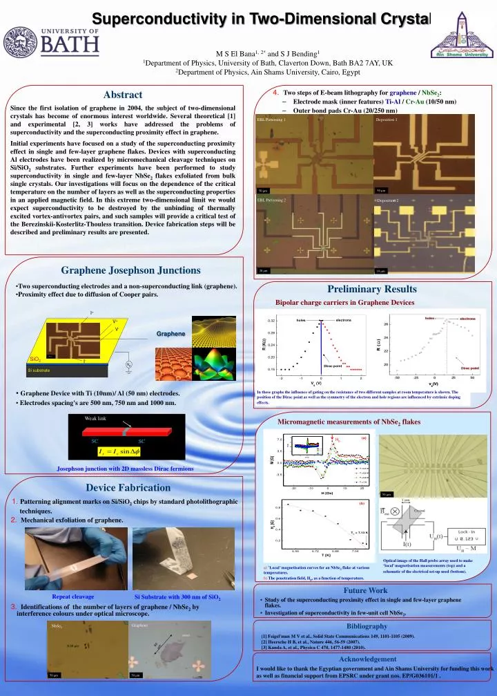
V g. EBL Patterning 1. Deposition 1. 50 μm. 50 μm. EBL Patterning 2. Deposition 2. 20 μm. 10 μm. H p. Optical image of the Hall probe array used to make ‘local’ magnetisation measurements (top) and a schematic of the electrical set-up used (bottom).

E N D
Vg EBL Patterning 1 Deposition 1 50 μm 50 μm EBL Patterning 2 Deposition 2 20 μm 10 μm Hp Optical image of the Hall probe array used to make ‘local’ magnetisation measurements (top) and a schematic of the electrical set-up used (bottom). a) ‘Local’ magnetisation curves for an NbSe2 flake at various temperatures. b)The penetration field, Hp, as a function of temperature. NbSe2 6.33 μm Superconductivity in Two-Dimensional Crystals M S El Bana1,2* and S J Bending1 1Department of Physics, University of Bath, Claverton Down, Bath BA2 7AY, UK2Department of Physics, Ain Shams University, Cairo, Egypt Abstract Since the first isolation of graphene in 2004, the subject of two-dimensional crystals has become of enormous interest worldwide. Several theoretical [1] and experimental [2, 3] works have addressed the problems of superconductivity and the superconducting proximity effect in graphene. Initial experiments have focused on a study of the superconducting proximity effect in single and few-layer graphene flakes. Devices with superconducting Al electrodes have been realized by micromechanical cleavage techniques on Si/SiO2 substrates. Further experiments have been performed to study superconductivity in single and few-layer NbSe2 flakes exfoliated from bulk single crystals. Our investigations will focus on the dependence of the critical temperature on the number of layers as well as the superconducting properties in an applied magnetic field. In this extreme two-dimensional limit we would expect superconductivity to be destroyed by the unbinding of thermally excited vortex-antivortex pairs, and such samples will provide a critical test of the Berezinskii-Kosterlitz-Thouless transition. Device fabrication steps will be described and preliminary results are presented. • 4. Two steps of E-beam lithography for graphene / NbSe2: • Electrode mask (inner features) Ti-Al / Cr-Au (10/50 nm) • Outer bond pads Cr-Au (20/250 nm) Graphene Josephson Junctions • Two superconducting electrodes and a non-superconducting link (graphene). • Proximity effect due to diffusion of Cooper pairs. Preliminary Results Bipolar charge carriers in Graphene Devices I+ V+ V- Graphene SiO2 100 μm I- Si substrate • Graphene Device with Ti (10nm)/ Al (50 nm) electrodes. • Electrodes spacing's are 500 nm, 750 nm and 1000 nm. In these graphs the influence of gating on the resistance of two different samples at room temperature is shown. The position of the Dirac point as well as the symmetry of the electron and hole regions are influenced by extrinsic doping effects. Micromagnetic measurements of NbSe2 flakes Josephson junction with 2D massless Dirac fermions Device Fabrication 50 μm 1.Patterning alignment marks on Si/SiO2 chips by standard photolithographic techniques. Weak link 2.Mechanical exfoliation of graphene. SC SC Future Work Repeat cleavage • Study of the superconducting proximity effect in single and few-layer graphene flakes. • Investigation of superconductivity in few-unit cell NbSe2. Si Substrate with 300 nm of SiO2 3.Identifications of the number of layers of graphene / NbSe2 by interference colours under optical microscope. Bibliography Graphene [1] Feigel'man M V et al., Solid State Communications 149, 1101-1105 (2009). [2] Heersche H B, et al., Nature 446, 56-59 (2007). [3] Kanda A, et al., Physica C 470, 1477-1480 (2010). 60 μm Acknowledgement I would like to thank the Egyptian government and Ain Shams University for funding this work as well as financial support from EPSRC under grant nos. EP/G036101/1. 50 μm 50 μm