Download
1 / 6
60 likes | 507 Views
蕭特基箝位電晶體 ( Schottky -Clamped transistor). 班 級 : 碩研光電一甲 授課教師 : 鄒文正 老師 報 告 者 : 朱致彤. 2013/12/11. 目錄. 基本介紹 應用 實例 & 缺點 參考文獻. 基本介紹.

E N D
蕭特基箝位電晶體(Schottky-Clamped transistor) 班 級: 碩研光電一甲 授課教師: 鄒文正 老師 報 告 者: 朱致彤 2013/12/11
目錄 • 基本介紹 • 應用實例&缺點 • 參考文獻
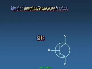
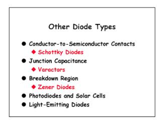
基本介紹 • 蕭特基箝位電晶體(Schottky-clamped transistor),是npn電晶體的基極與集電極之間加接有一個SBD(Schottky二極體)的BJT(如下圖)。其優點就是使得當BJT進入飽和狀態時,其集基電壓Vbc被箝位在SBD的導通電壓(≈0.25V)上,從而避免了BJT進入深飽和狀態,減小了超量少子存儲電荷,則可減短BJT開關過程中的存儲時間(可縮短1個數量級),導致集成電路中的信號傳輸延遲時間大大減短(延遲時間可降低到2~4ns,延遲時間與功耗的乘積大約可降低一半),結果可提高集成電路的工作速度。SCT是製作高速數字集成電路的基本器件。 Fig.1. 蕭特基箝位電晶體示意圖[1]
應用實例&缺點 • 在傳輸延遲時間與功耗的乘積一定時,採用SCT可設計兩種TTL電路: (a)保持功耗不變,使傳输延遲時間减短—高速TTL(STTL) (b)保持傳输延遲時間不變,使功耗降低—中速低功耗TTL(LSTTL) • ① SBD的接入使得BJT的飽和壓降升高。② 使得BJT的反向漏電流增大。③ 技術成分高(對於Si的表面處理和金屬化技術要求很高,而且重複性和可靠 性較差)等。
參考文獻 • 維基百科,Schottkytransistor • 半導體元件物理,施敏