Download
1 / 27
270 likes | 403 Views
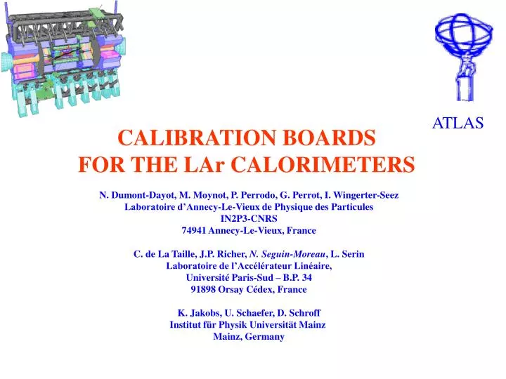
ATLAS. CALIBRATION BOARDS FOR THE LAr CALORIMETERS. N. Dumont-Dayot, M. Moynot, P. Perrodo, G. Perrot, I. Wingerter-Seez Laboratoire d’Annecy-Le-Vieux de Physique des Particules IN2P3-CNRS 74941 Annecy-Le-Vieux, France C. de La Taille, J.P. Richer, N. Seguin-Moreau , L. Serin

E N D
ATLAS CALIBRATION BOARDSFOR THE LAr CALORIMETERS N. Dumont-Dayot, M. Moynot, P. Perrodo, G. Perrot, I. Wingerter-Seez Laboratoire d’Annecy-Le-Vieux de Physique des Particules IN2P3-CNRS 74941 Annecy-Le-Vieux, France C. de La Taille, J.P. Richer, N. Seguin-Moreau, L. Serin Laboratoire de l’Accélérateur Linéaire, Université Paris-Sud – B.P. 34 91898 Orsay Cédex, France K. Jakobs, U. Schaefer, D. Schroff Institut für Physik Universität Mainz Mainz, Germany
OUTLINE • ATLAS LAr CALORIMETER READOUT • REQUIREMENTS • HISTORY • ANALOG and DIGITAL DMILL CHIPS • 8 CHANNELS BOARD • 128 CHANNELS BOARD N. Seguin-Moreau, 8th conference on LHC elctronics, COLMAR
ATLAS Lar EM calorimeter readout Calibration : 116 boards @ 128 ch Front End Board (FEB) : 1524 boards @ 128 ch Electrodes Cold to warm Feedthrough Front End Crate: Readout and Calib. signals CALIB. FEB TBB Controller Cryostat
CALIBRATION: Requirements and Principle • Goal: Inject a precise current pulse [Ical] as close as possible as the detector pulse • Rise time < 1ns . • Decay Time around 450 ns . • Dynamic range : 16 bits (100 μV to 5V) . • Integral non linearity < 0.1% . • Uniformity between channels better than 0.25%(to keep calorimeter constant term below 0.7%) • Timing between physics and calibration pulse ±1ns • Operation in around 100 Gauss field • Radiation hardness: • 50 Gy, 1.6 1012 Neutrons/cm2 in 10 years • Taking account safety factors, DMILL chips must be qualified up to 500 Gy, 1.6 1013 Neutrons/cm2 • Run at a few kHz PULSER ROOM T LAr HF SWITCH 0.1% Rinj N. Seguin-Moreau, 8th conference on LHC elctronics, COLMAR
HISTORY • 12 boards produced in 1998 with COTS [LEB98 and LEB99] • 5 years successful operation in beam tests. Problems were mainly chips badly soldered and dead transistors, but • Radiation tolerance: • Inadequate with COTs that failed irradiation tests at 20 Gy • Chips migration to DMILL technology • Improve parasitic signal at DAC=0: • About 1.2 GeV equivalent (3 % of the high gain range) • HF switch redesigned with a PMOS transistor instead of 4 PNPs transistors in parallel: 10 times improvement • Delay chip linearity and monotony marginal (and strongly dependent on power supply) • DAC time stability improvement • Digital part: to be simplified, 10 ALTERAs removed and replaced by DMILL ASICs. N. Seguin-Moreau, 8th conference on LHC elctronics, COLMAR
128 CHANNELS CALIBRATION BOARD : ANALOG PART • A low offset op. amp. distributes the DAC voltage to the 128 channels. • One low offset op.amp. per channel generates the calibration current through a 5W [0.1%]. V to I conversion V follower 5 W 0.1% Low Off Op Amp HF Switch Vout: 50 μV to 5V in 25 W 16 bits DAC 128 channels calibration board Idc: 2uA to 200 mA N. Seguin-Moreau, 8th conference on LHC elctronics, COLMAR
16 bits DMILL DAC: requirements and design • 16 bits dynamic range (16 μV-1V), accuracy 0.1% • Good stability at small DAC value • External R/2R ladder and highly degenerated current sources • DAC DMILL: V1 and V2 (Different Iref) • Bandgap reference voltage (1.5 V) or external voltage • DAC V2: Submitted in Sept 01, area : 8 mm2 • 123 received in May 02, yield : 90% DAC V2 16 I sources DAC V2 External 0.1% R Iref Bandgap V to I convertor External 0.1% degener. R N. Seguin-Moreau, 8th conference on LHC elctronics, COLMAR
0.01% 0.01% 0.01% DAC performance : Linearity • DC measurement performed with precise multimeter • Measurement performed with the Bandgap reference • Accuracy: 0.01 % or 10 μV • INL < 0.01%:explained by single bit linearity N. Seguin-Moreau, 8th conference on LHC elctronics, COLMAR
Irradiation results: shown at LEB7 (Stockholm) Temperature stability (with the bandgap reference) measured on 1 DAC V2: better than -0.01%/K Due to R and Isources temperature sensitivity Time stability measured DACs V1 Bit0 ON Bit15 ON - 51 μV/K 0.02% 25 47 Temperature 15 h DAC performance Vdac with all the bits ON (DAC V2) N. Seguin-Moreau, 8th conference on LHC elctronics, COLMAR
Offset around 16mV[DAC LSB] or less . Offset stable in time Temperature sensitivity :0.1%or 1 LSB for 10°C Integral non linearity < 0.1% . Speed not crucial: Settling time < 100 ms Input range: from 5 V to 4 V Output range: DC current from2mA to 200mA Pulse Out: 50 mV to 5Vin Zout=25 W Power supplies: Op Amp: VDD= +7VandVss= +2V. V to I conversion V follower DAC HF Switch DMILL LOW OFFSET Op Amp: Requirements N. Seguin-Moreau, 8th conference on LHC elctronics, COLMAR
Low offset op amp design • Used in 0.2% accuracy DC current source (2 μA-200 mA) (Orsay) 5 W 0.1% External 165kW 0.1% collector resistors Enable input Second stage : 1000/1.2 cascoded diff. pair DAC in External R: Window of trimming Centroid bipolar diff. Pair 10/1.2 Output PMOS : 20,000/0.8 for IDAC=200mA External compens. 1 nF to VP6 Current out Fuses for fine offset trimming to ± 10 μV N. Seguin-Moreau, 8th conference on LHC elctronics, COLMAR
Low offset op amp versions • First version in 0.8μm BICMOS AMS technology in 2000 • Selection inside ±200 μV => 23/24 Op amps=95 % • First DMILL chip: Op Amp V1 • Op Amp design: minor modifications compared to the AMS version • 40 chips received in Feb 01. Area = 1.82 mm2 • Ceramic package JLCC28 • 3 not working • Selection inside ±200 μV => 32/37 Op amps=86 % • Final version V2 • Include HF switch (cost reduction) • Op amp: identical as V1 • Chip submitted in May 01. Area : 3 mm2 • Plastic package PQFP44 Layout of Op Amp V1 1960*1460 Layout of Op. Amp. V2 N. Seguin-Moreau, 8th conference on LHC elctronics, COLMAR
Yield : 593 chips received Nov 01. 574 Fully functional, 19 out of working →Yield : 96% Selection inside ±200 μV : 364 Op Amp →sorting yield : 63.4% Example of offset trimming: Op Amp performance: Offset Op Amp trimmed down to –7 μV Initial Offset:–254 μV N. Seguin-Moreau, 8th conference on LHC elctronics, COLMAR
Op Amp performance • Irradiation tests : Performed on V1 and shown at LEB7 (Stockholm) • DC Linearity: DC output current measured with a precise multimeter. • Offset not sensitive to the DAC value Residuals in µV N. Seguin-Moreau, 8th conference on LHC elctronics, COLMAR
Time stability (10 Op Amps) Output DC current monitored Stability better than 10mV Temperature stability (10 Op Amps) Largest variation (<2 mV/degree) for OA with the largest initial offset 10 chips previously trimmed down to a few mV kept at 87 degree during 4 days. Stability found better than 2 mV over this period. Offset stability: Offset variation 5 mA or 25 mV 40 mV 25 ° 50 ° 90 minutes N. Seguin-Moreau, 8th conference on LHC elctronics, COLMAR
OP AMP PRODUCTION AND TEST • 28000 op amps produced before the end of 2002 • Use of the Grenoble robot to test them and trim op amps with offset < ± 200 µV • DC measurements for 3 DAC values: • Total Offset (in+-in-) • DV Rc (2nd stage offset) • IDC out after PMOS Switch • Check 7.5 V Power Consumption N. Seguin-Moreau, 8th conference on LHC elctronics, COLMAR
DIGITAL PART SPAC: I2C frame I2C CALOGIC (LAPP Annecy): Generate calib. Window and reset signals SPAC I2C Clock40 TTCrx TTCRx: ATLAS TTC commands CALOGIC Reg0-3: 32 bits R/W register To enable the 128 ch. DAC REG REG0 REG1 TTC decode REG2 REG3 16 32 32 32 32 CALOGIC: 16 bits R/W reg. To load the DAC value Delay0 Delay1 4 4 16 bits DAC DELAY (CERN): 0-24 ns, step 1ns 16 Pulsers 16 Pulsers 16 Pulsers 16 Pulsers 16 Pulsers. 16 Pulsers 16 Pulsers 16 Pulsers ANALOG PART N. Seguin-Moreau, 8th conference on LHC elctronics, COLMAR
Control logic : DMILL (ANNECY) Common DMILL chip to control DAC, pattern and delays registers and to decode TTCRx commands. 16 mm2 chip, received 39 (MPW 05/01).Yield : 100% Irradiation tests SEE test performed in Feb 02 (Louvain) no SEU up to ~8 1012 p+ (60 MeV) In ATLAS < 2 SEU/yr Pattern Pattern register (32 bits) SCL SDA CalibIn Calib counter (11 bits) I2C Function Select Reset register Clock40Des1 TTCrx decoding Command ResetIn PowerOn Reset CalibOut Autozero ResetOut Digital chips: CALOGIC N. Seguin-Moreau, 8th conference on LHC elctronics, COLMAR
Delay chip : DMILL (CERN) To align physics signal and calibration pulse 4 delay lines/chip 0-24 ns, 1ns step Linearity residuals: ±60 ps Jitter = 25 ps SEE test performed in Feb 02 (Louvain) 4 chips monitored One error occurred, cleared by power reset Digital chips: DELAY Residuals (ns) Jitter + 60 ps 22 ps - 60 ps N. Seguin-Moreau, 8th conference on LHC elctronics, COLMAR
8 channels prototype towards the 128 channels board • Board very different from Module 0 • Channels no longer aligned but staggered in depth • Difficult tuning • Ground bounce • 2V change with enabled channels • 80 µV DAC offset • DAC change with all channels on • Overshoot • Signal uniformity • DC uniformity • Damaged chips • Oscillations • Ripple noise • Linearity • But all hopefully fixed! 8 channels module Module 0 128 channels board SPAC2 DAC Calolgic TTCRx Delay 8 Opamps & switches 8 outputs N. Seguin-Moreau, 8th conference on LHC elctronics, COLMAR
Pulse shape before shaping • Full DAC range • 100 µV 1V • Up to 5V pulses in 50 Ω • Rise time • < 2 ns • Very small variation with DAC • Undershoot • Due to 50 Ω line between the switch and R0: should be 25 Ω • Will be corrected • HF Ringings: • At small DAC values, due to parasitic package inductance DAC=100 µV DAC=1 mV 0dB DAC=10 mV 0dB DAC=0.1V -20dB DAC=1V -40dB N. Seguin-Moreau, 8th conference on LHC elctronics, COLMAR
Pulse shape after shaping • Parasitic injected charge • Peak of Qinj: • Equivalent to DAC=30 µV • At signal peak : • Qinj< DAC = 15 µV • Improvement by >10 compared to module 0 Qinj DAC=0µV DAC=100µV 0dB DAC=1mV -20dB DAC=1V -80dB N. Seguin-Moreau, 8th conference on LHC elctronics, COLMAR
CH7 : VB=+5V DAC=1mV -20dB Parasitic Injected Charge (PIC) Improvement • Improvement : • CH7 had the Nwell tied to 5V, as in the original configuration. • Nwell of the other channels connected to the PMOS source to reduce the ringings => Clear improvement of Qinj • On 8 channels • Good uniformity of the PIC N. Seguin-Moreau, 8th conference on LHC elctronics, COLMAR
DC and Pulse Linearity Gain 100 Gain 10 • Measured on 3 gains 1-10-100 • Pulse measurements • In red • After shaping (tp=50ns) • DC current measur. • In black • With Keithley • Example of problems • DAC referenced to VP6 by mistake • Bad 5Ω resistor brand • Dynamic performance at the level to DC performance Pulse Linearity Residuals +0.05% +0.05% -0.05% -0.05% Dc Linearity Residuals Gain 1 Gain 1 DC linearity +0.1% +0.05% Dac Ref corrected Bad R replaced -0.05% -0.1% N. Seguin-Moreau, 8th conference on LHC elctronics, COLMAR
Designing the 128ch board • 16 times replication of the 8 channels module • Many tricky PCB layout details: to avoid coupling between digital and sensitive analog signals • Difficult VP6 Distribution • Connection between 5Ω and ref. VP6 taken for the DAC • Must be uniform for all channels within 0.1% • Can’t be shared between channels tominimize variation of amplitude with number of enabled channels • Star configuration mandatory • All VP6 lines equalized in length • Common reference point on board center : dimension 2 x 1 cm = 1 mΩ => 5 layers necessary for the VP6 routing VP6 ref DAC 150 mm 220 mm N. Seguin-Moreau, 8th conference on LHC elctronics, COLMAR
128 channels PCB layout • C5 layer: • Top layer : analog components • Bottom layer: Digital components N. Seguin-Moreau, 8th conference on LHC elctronics, COLMAR
CONCLUSION • 2 prototypes of 128 channels calibration boards ready for tests of final ATLAS calorimeter electronics next october (1/2 crate) • Production of 130 boards for ATLAS: • Call for tenders at the beginning of 2003 • Chips production • DELAYS (600 already produced) • DAC, SPAC, CALOGIC: to be produced on the same digital wafer in 2003 • OP AMPs (28 000 to be produced before the end of 2002) N. Seguin-Moreau, 8th conference on LHC elctronics, COLMAR