Download
1 / 48
500 likes | 692 Views
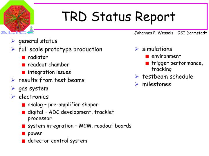
TRD Status Report. Johannes P. Wessels – GSI Darmstadt. general status full scale prototype production radiator readout chamber integration issues results from test beams gas system electronics analog – pre-amplifier shaper digital – ADC development, tracklet processor

E N D
TRD Status Report Johannes P. Wessels – GSI Darmstadt • general status • full scale prototype production • radiator • readout chamber • integration issues • results from test beams • gas system • electronics • analog – pre-amplifier shaper • digital – ADC development, tracklet processor • system integration – MCM, readout boards • power • detector control system • simulations • environment • trigger performance, tracking • testbeam schedule • milestones
General status • September `01 - technical design report submitted • November `01 – presented to the LHCC • January `02 – recommended for approval by LHCC • February `02 – approved by Research Board • because of the funding situation -> recommendation to build `short asymmetric´version (about 58%) Actively seeking funds at the moment; Japanese have expressed interest to join the project and are in the process of requesting support.
Chamber design pad plane with HEXCELL/CF backing amplification region drift region radiator
First pad plane support • Polish manufacturer (LHCb) • bottom side: flatness better than 100 microns • top side: flatness better than 300 microns • tolerances well within needs
First pad planes • size of ordered pieces: 1200 x 512 mm2 (200 µm thickness) • need 3-4 pieces/chamber depending on length of chamber • manufactured by OPTIPRINT, Switzerland • still problems with handling
Bending of pad plane support • sandwich with aluminum frame taped to flat table • measurement of deflection of center and sides as function of overpressure • sandwich deforms exactly as calculated using a simple model for sandwich structures • maximum bending with respect to anode wires <220microns
Expected gas gain variation • gain varies linearly with bending of pad plane • for the maximum tolerated overpressure in the chamber about 15% gain variation is expected • additional wire sag not important for a large range in cathode wire tension
Radiator • CF-laminated `quilt´ structure of: • 100 micron CF laminate • Rohacell HF71 • polypropylene fibers from Freudenberg LRP375BK • optimization of ROHACELL vs fiber thickness ongoing • have option to buy stock retained for Aachen for prototype developments • full production for ALICE TRD will be 80k€
Material for prototypes • goal is to build fully functional prototypes • Polish CFK/HF71 (8mm) and 7 layers LRP375BK - radiator finished including electrode - now testing for wire load and overpressure • AIK CFK/HF71 (8/6 mm) 7/8 layers LRP375BK - CFK on hand, fibers arrive by mid-April • Polish CFK/HF71 (6mm) with 8 layers LRP375BK - need to purchase raw materials and place order Polish manufacturer provides thinner, smoother, and cheaper laminate – BUT sole supplier issue
Radiator detail • 8mm ROHACELL HF71 coated with ~ 100 micron CF covered mith Al-Mylar • partially filled with Freudenberg fibers LRP375BK (ATLAS)
Full size radiator laminated material purchased – radiator assembly by Muenster group
Detail during chamber assembly assembly of first full scale prototype done in Heidelberg
Full scale prototype largest chamber: 1200 x 1600 mm
Winding machine • machine currently under test at GSI • tensioning mechanism conditioned • full-size transfer frames delivered • will be moved to Heidelberg in April
Influence of wire tension on frames • deformation of sides about 130µm each • corresponds to maximum relaxation of wire tension by 13% red line denotes load according to TDR
Gas feed-through - design 2 feed throughs per chamber 10 chambers per circuit pressure drop for 10 chambers < 0.05 mbar
Gas feed-through • leakage has been tested • with small prototypes • misalignment of chambers • was pushed to 4 degrees • between faces • at 10l/h flow and 10ppm oxygen -> full TRD would loose 0.027l/h due to seals (TDR < 0.5l/h) • approx. 1000 CHF/yr
Rollers • rollers now attached to L-profiles welded to space frame • reduces space necessary for support • increases stiffness of thin supermodules • same gadgets needed on installation tool
Results from 2001 testbeam • resolution of the `good´ xenon - `bad´ xenon story • momentum scan to evaluate pion rejection for various compositions of radiator materials • position resolution and angular resolution for tracking
Good Xenon – Bad Xenon • different bottles of Xe show very different average pulse height distributions in drift region • finally managed to resolve this long-standing problem • traced to minuscule contaminations of VERY electronegative components • <0.1ppm CF4 • 0.08ppm C2F6 • 0.8ppm O2 • 0.68ppm SF6 (!) • suppliers now aware of this
Status of gas system • test system with purification and recuperation operational • molecular sieves retain CO2 • because of small volumes used so far, recuperation only performed off-line • test system modified; now includes buffer vessel for regulating small volumes (compressor can handle full detector -> 27m3) • system including recuperation will be used in the stack test in Fall 2002
Pion efficiency • CERN measurements scaled to reproduce GSI data at 1 GeV/c for identical radiator • pion sample still contains some (soft?) electrons (next slide) • pion rejection shown to not deteriorate for higher momenta • thick carbon fiber laminate 300 microns decreases rejection by factor 2-3. Still at 1% in relevant momentum range • new production uses only about 100 microns
Electron pion spectra Data (CERN T10 + GSI) Simulation + Data - GSI
Tracking resolution • ALICE operational point at S/N = 30-40 • difference in angular resolution is an artifact due to slightly different length of the drift region in the two test chambers
Tracking resolution (B-field) • test setup at GSI with large coils • soft delta electrons curl up in magnetic field • improved point and angular resolution
Lorentz angle for Xenon • exact knowledge of Lorentz angle necessary for precise track reconstruction • data in literature not consistent • within limits posed by the precise knowledge of the CO2 content values agree with MAGBOLTZ
Preamplifier status • 3rd chip submitted end of January • expected back end of March • possibly last iteration • increased size due to fully differential design
Footprint of preamplifier • 18 fourth order pre-amp shapers with differential outputs (21) • external references to adjust to range of ADCs • digital test structure for chip verification • size of chip: 3030 µm x 7280 µm
Evaluation of PASA • complete evaluation prepared; chip expected back in two weeks • some results from simulations • full signal in center channel • 50% signal in adjacent pads -> produces cross talk on <10-5 level in neighboring channels • full corner analysis • only small yield expected outside specifications (mainly leading to too short shaping time) • gain variations tolerable
Digital chip - recent changes & developments • Conceptual Design Review conducted in early January • complete design now for 0.18µm UMC process • tail cancellation network now baseline design • link width reduced to D8+P+Spare double data rate • giving up on dynamic error correction (Hamming) • implementation of one spare signal allowing to multiplex out stuck bits (maximum 2 per link) • readout tree simplified • configuration tree fully operable in FPGAs (2 nodes tested; currently implementing Linux interface) • MIMD CPU (1 node) operable in FPGA • FPGA CPU boots UCLinux for Slow Control • LVDS Rx and Tx implement power down mode now (wake-up time ~500 ps) • use of ALTRO chip as 16-channel ADC from TPC (test/fall back)
ADC – Univ. Kaiserslautern Parameter Value Sampling Rate 10 MSpS Resolution 10 Bits Power Consumption 5 mW Max. INL 1 LSB Input signal BW 5 MHz Diff. Input Range +/- 1V Chip Area 0.2 mm² Converter Principle cyclic
S S S S N N N N N N N N N N G V T T T T G V G V G V G V G V G V E E E E I I I I I I I I I I N C C M D D N C N C N C N C N C N C R R R R _ _ _ _ _ _ _ _ _ _ D C K S I O D C D C D C D C D C D C 0 0 0 0 P P P P P P P P P P _ _ _ _ 0 0 0 0 0 0 0 0 0 0 D D D D _ _ _ _ _ _ _ _ _ _ O O I I P P S S C C D D D D U U N N R R T T T T 9 9 8 8 - + - + - + T T E E R R R R - + o o B B L L - + - + - + N N N O R N N S S S S N N N N N N N N N N N N N N N N N N N N U E E E E I I I I I I I I I I I I I I I I I I C C C S C C C C T R R R R _ _ _ _ _ _ _ _ _ _ _ _ _ _ _ _ _ _ T _ 1 1 1 1 P P P P P P P P P P P P P P P P P P _ R _ _ _ _ 1 1 1 1 1 1 1 1 1 1 1 1 1 1 1 1 0 0 n D D D D _ _ _ _ _ _ _ _ _ _ _ _ _ _ _ _ _ _ N G O O P P S S C C I I D D D D D D D D D D D D N N 9 9 8 8 7 7 6 6 5 5 7 7 U U R R T T T T T T - + E E R R R R - + - + - + - + - + - + - + o o B B L L - + - + - + VCC GND NI_P0_ D5+ NI_P0_ D5- VCC GND NI_P0_ D4+ NI_P0_ D4- VCC GND NI_P0_ D3+ VCC PLL_LOC KED NI_P0_ D3- GND PLL_RE SET VCC CLK_PLL _IN SEL_C LK GND CLK_PLL _IN PA_SS TR NI_P0_ D2+ VCC PA_SC LK NI_P0_ D2- GND PA_SD AT NI_P0_ D1+ ADCM0 _D9 ADCM0 _D8 NI_P0_ D1- ADCM0 _D7 ADCM0 _D6 VCC ADCM0 _D5 ADCM0 _D4 GND ADCM0 _D3 ADCM0 _D2 NI_P0_ D0+ VCC ADCM0 _D1 NI_P0_ D0- ADC_C LK ADCM0 _D0 VCC GND ADCM2 _D0 GND ADCM2 _D1 ADCM2 _D2 NI_P0_C LKo+ ADCM2 _D3 ADCM2 _D4 NI_P0_C LKo- ADCM2 _D5 ADCM2 _D6 VCC ADCM2 _D7 ADCM2 _D8 GND VCC ADCM2 _D9 NI_P4_C LKi+ GND ADCM3 _D8 NI_P4_C LKi- ADCM3 _D9 ADCM3 _D6 VCC ADCM3 _D7 ADCM3 _D4 GND ADCM3 _D5 ADCM3 _D2 NI_P4_ D0+ ADCM3 _D3 ADCM3 _D1 NI_P4_ D0- VCC ADCM3 _D0 VCC GND ADCM1 _D0 GND ADCM1 _D1 ADCM1 _D2 NI_P4_ D1+ ADCM1 _D3 ADCM1 _D4 NI_P4_ D1- ADCM1 _D5 ADCM1 _D6 VCC ADCM1 _D7 GND VCC GND ADC_S EL0 N N N N N N N N N N N N N N N N N N N N N N N N N N N N N N N N N N N N N N N C I I I I I I I I I I I I I I I I I I I I I I I I I I C I I C I I C I I I I C _ _ _ _ _ _ _ _ _ _ _ _ _ _ _ _ _ _ _ _ _ _ _ _ _ _ _ _ _ _ _ _ _ _ P P P P P P P P P P P P P P P P P P P P P P P P P P P P P P P P P P 3 3 3 3 3 3 3 3 3 3 3 3 3 3 3 3 3 3 3 3 3 3 3 3 3 3 3 3 2 2 2 2 2 2 _ _ _ _ _ _ _ _ _ _ _ _ _ _ _ _ _ _ _ _ _ _ _ _ _ _ _ _ _ _ _ _ _ _ P P S S C C C C C C D D D D D D D D D D D D D D D D D D D D D D D D 9 9 8 8 7 7 6 6 5 5 4 4 3 3 2 2 1 1 0 0 0 0 1 1 R R T T T T L L L L E E R R R R - + - + - + - + - + - + - + - + - + - + K K K K - + - + o o B B L L o o o o - + - + - + - + - + G V N N N N G V N N G V N N G V N N N N G V N N G V N N N N G V N N G V N N G V N C I I I I N C I I N C I I N C I I I I N C I I N C I I I I N C I I N C I I N C D C _ _ _ _ D C _ _ D C _ _ D C _ _ _ _ D C _ _ D C _ _ _ _ D C _ _ D C _ _ D C P P P P P P P P P P P P P P P P P P P P P P 4 4 4 4 4 4 4 4 4 4 4 4 4 4 4 4 4 4 4 4 4 4 _ _ _ _ _ _ _ _ _ _ _ _ _ _ _ _ _ _ _ _ _ _ P P S S C C D D D D D D D D D D D D D D D D R R T T T T 9 9 8 8 7 7 6 6 5 5 4 4 3 3 2 2 - + - + - + - + - + - + - + - + E E R R R R i i B B L L - + - + - + PAD layout of TRAP1 chip A DC P LL NI_P0_ D6+ Input port NI_P0_ D6- NI_P1_ D4+ EAST NI_P1_ D4- NI_P1_ D3+ NI_P1_ D3- NI_P1_ D2+ NI_P1_ D2- Input port NI_P1_ D1+ NI_P1_ D1- H NI_P1_ D0+ NI_P1_ D0- NC T NI_P1_C LKo+ NI_P1_C LKo- U NC H NI_P2_P REo+ NI_P2_P REo- O NI_P2_S TRB+ T NI_P2_S TRB- S NI_P2_C TRL+ NI_P2_C TRL- R NI_P2_ D9+ Input port NI_P2_ D9- O NI_P2_ D8+ NI_P2_ D8- NI_P2_ D7+ N NI_P2_ D7- NI_P2_ D6+ NI_P2_ D6- NI_P2_ D5+ NI_P2_ D5- NI_P2_ D4+ NI_P2_ D4- NI_P2_ D3+ NI_P2_ D3- NI_P2_ D2+ NI_P2_ D2- NC ADCM1 _D8 ADCM1 _D9 WEST ADC_S EL1 • total area 25mm2 • 32 power/GND pads • merger MCMs require only single pad ring Input port Output port
MIMD Processor screen shot of full layout of MIMD processor
MCM footprint • contains 18ch preamp 21 ADCs (ALTRO) tracklet processor controls • BGA432 package • 432 pins (4 rows, 31 pads) • grid 1.27mm x 1.27 mm • dimensions roughly 40x40 mm2 • few external components
Status of simulation software • geometry follows latest design • detailed geometry of MCMs and cooling included • supermodule support structure included; rails, services soon to come • hit compression from TPC included • tilted pad option included • adapted pad response functions • time response function included • digital filter tail cancellation included MCM detail
New digits display available allows to superimpose digits from different events
Tracking • trigger performance now checked for tilted pads • fast simulations -> parameterization of response will done • global tracking strategy for all detectors IST, TPC, TRD now using Kalman filter • still some problems with tilted pads • for electrons special treatment of Bremsstrahlung needs to be implemented • electron identification and pion rejection using transition radiation and dE/dx signals need to be provided for electron tracking strategy
Future use of testbeams • 2002 – 12 days (performance) • stack test (at least three layers) • momentum dependence of pion rejection • final preamp and tracklet processor on MCM • final gas system • cooling and DCS test systems • 2004 – 8 days (1/2 calibration, 1/2 quality assurance) • several full stack tests • high statistics measurement of pion and electron spectra up to highest momenta (6 GeV/c) • test of global tracking unit (GTU) • test of calibration scheme • 2003 – 9 days (1/3 performance, 2/3 quality assurance) • full stack test – multi-hit capability • trigger performance evaluation • test of readout system • check of cooling and DCS systems • 2005 – 7 days (calibration) • calibration of several stacks including full momentum scan • commissioning of GTU
Milestones • 12-01: digital chip engineering design review • done in January; concept considered appropriate yet challenging; some suggestions already incorporated for submission • 01-02: 3rd MPW run submission of PASA • date has been met, chips expected back in about two weeks • 04-02: 1st submission of digital chip TRAP1 • actual submission date will be April, 17; contains track let processor, 3 ADCs, configuration tree, separate inputs for use with external ADCs • 05-02: engineering design review of chamber design • foreseen for end of May; date can be met if all pending tests go well Dates for production milestones will need to be revisited if change in overall schedule will be announced