
Uploaded by
perry-schwartz
6 SLIDES
215 VIEWS
70LIKES
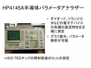
HP4145A 半導体パラメータアナラザー
DESCRIPTION
HP4145A 半導体パラメータアナラザー. ダイオード、トランジスタなどの電子デバイスの各種の直流特性を正確に測定 グラフ表示、パラメータ解析が可能. ⇒SOI TEG チップの照射前後の V D, I D の測定. GPIB で制御 V1:0 ~ 2V ,step0.1V V2: 測定. V1=Vs1. 47kΩ. V2=Vm1. 47kΩ. SMU(Source Monitor Units) を用いた測定. source V (SMU1) V: -0.5 ~ 1(V) step 0.01(V) I (SMU1): 測定
Download
1 / 6
Download Presentation 
HP4145A 半導体パラメータアナラザー
An Image/Link below is provided (as is) to download presentation
Download Policy: Content on the Website is provided to you AS IS for your information and personal use and may not be sold / licensed / shared on other websites without getting consent from its author.
Content is provided to you AS IS for your information and personal use only.
Download presentation by click this link.
While downloading, if for some reason you are not able to download a presentation, the publisher may have deleted the file from their server.
During download, if you can't get a presentation, the file might be deleted by the publisher.
E N D
Presentation Transcript
HP4145A半導体パラメータアナラザー • ダイオード、トランジスタなどの電子デバイスの各種の直流特性を正確に測定 • グラフ表示、パラメータ解析が可能 ⇒SOI TEGチップの照射前後のVD,IDの測定
GPIBで制御 V1:0~2V ,step0.1V V2:測定 V1=Vs1 47kΩ V2=Vm1 47kΩ
SMU(Source Monitor Units)を用いた測定 source V (SMU1) V: -0.5 ~ 1(V) step 0.01(V) I (SMU1):測定 compliance 100μA SMU1 V,I A Diode or module SMU2 Com
各moduleの10μA付近での抵抗値 ・modeleの抵抗値 2~3.5kΩ ・50kΩを超えるものはない
More Related
Audio
Live Player