Download
1 / 1
10 likes | 144 Views
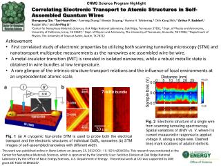
CNMS Science Program Highlight. Correlating Electronic Transport to Atomic Structures in Self-Assembled Quantum Wires Shengyong Qin , 1 Tae-Hwan Kim , 1 Yanning Zhang, 2 Wenjie Ouyang, 2 Hanno H. Weitering, 3 Chih -Kang Shih, 4 Arthur P. Baddorf , 1 Ruqian Wu, 2 and An-Ping Li 1

E N D
CNMS Science Program Highlight Correlating Electronic Transport to Atomic Structures in Self-Assembled Quantum Wires Shengyong Qin,1Tae-Hwan Kim,1Yanning Zhang,2Wenjie Ouyang,2 Hanno H. Weitering,3Chih-Kang Shih,4Arthur P. Baddorf,1 Ruqian Wu,2 and An-Ping Li1 1Center for Nanophase Materials Sciences, Oak Ridge National Laboratory, Oak Ridge, Tennessee 37831; 2Dept. of Physics and Astronomy, University of California, Irvine, CA 92697; 3 Dept. of Physics and Astronomy, The University of Tennessee, Knoxville, TN 37996; 4 Department of Physics, The University of Texas at Austin, Austin, TX 78712 40 pS 7-wire bundle 0 pS • Achievement • First correlated study of electronic properties by utilizing both scanning tunneling microscopy (STM) and nanotransportmultiprobe measurements as the nanowires are assembled wire-by-wire. • A metal-insulator transition (MIT) is revealed in isolated nanowires, while a robust metallic state is obtained in wire bundles at low temperature. • A rare glimpse of the intrinsic structure-transport relations and the influence of local environments at an unprecedented atomic scale. 20 nm Fig. 2 Electronic structure of a single wire from scanning tunneling spectroscopy. Spatial variations of dI/dV vs. V, where I is current measured in response to applied voltage V, along a single wire. Dashed lines mark locations of adatom defects. • Fig. 1 (a) A cryogenic four-probe STM is used to probe both the electrical transport and the electronic structures of individual GdSi2 nanowires (b) STM images of self-assembled nanowires with different width. This work was published online in Nano Letters on January 23, 2012 DOI: 10.1021/nl204003s. This research was conducted at the Center for Nanophase Materials Sciences, which is sponsored by the Scientific User Facilities Division at Oak Ridge National Laboratory by the Office of Basic Energy Sciences, U.S. Department of Energy. Theoretical work at UCI was supported by DOE grant DE-FG02-05ER46237.