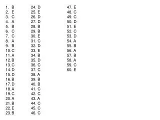
Download
1 / 25
250 likes | 310 Views
Contents. Structure of clean Si(5 5 12)-2 1 Steps and kinks on clean Si(5 5 12)-2 1 Growth of Ag nanowires on Si(5 5 12)-2 1. Growth and disorder of Ag nanowires on Si(5 5 12)-2 1 surface. J.Zhang a , S.H.Cho b , and J.M.Seo b

E N D
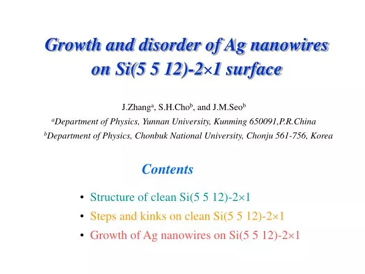
Contents • Structure of clean Si(5 5 12)-21 • Steps and kinks on clean Si(5 5 12)-21 • Growth ofAg nanowires on Si(5 5 12)-21 Growth and disorder of Ag nanowires on Si(5 5 12)-21 surface J.Zhanga, S.H.Chob, and J.M.Seob aDepartment of Physics, Yunnan University, Kunming 650091,P.R.China bDepartment of Physics, Chonbuk National University, Chonju 561-756, Korea
001 113 117 119 1111 1113 1115 115 113 115 117 118 116 112 114 113 337 3311 115 3313 335 3317 30.5 113 225 227 114 223 112 229 0 5513 5519 5517 557 5511 559 113 338 337 113 334 3310 335 112 7717 7715 779 7711 7713 7719 113 4411 112 449 225 445 223 447 9923 337 9917 9919 9911 9913 335 5512 559 556 558 112 5511 557 (hhk) degree L(nm) 001 0 0.36 225 29.5 2.21 771730.23.78 5512 30.55.35 337 31.2 1.57 (5 5 12) = (337) x 2 + (225) (7 7 17) = (337) + (225) 111 30.5 54.7 Side view of the silicon crystal lattice between the (001) and (111) planes
dimer dimer (5 5 12) [-110] [66-5] (7 7 17) Structural model of Si(5 5 12)-2×1 surface
[ 1 1 0 ] STM images of clean Si(5 5 12)-2×1 surface Tetramer 21 unit cell 0.77×5.35nm π-chains [ 6 6 5 ] [ 6 6 5 ] [ 1 1 0 ] Error signal 200Å×200Å Topography 200Å×200Å • Reconstruction: Cooling down at ~2 C /sec. from 700 C to RT • Filled-state STM image: I= 0.6nA, Bias = -2.5V, Rotation= 30
200Å×200Å tetramers (5 5 12) (225) (337)’ (337) extra(337) -chains (7 7 17) [ 1 1 0 ] adsorbed dimers [ 6 6 5 ] 3-D STM image of clean Si(5 5 12)-2×1 (5 5 12) = 2×(3 3 7) + (2 2 5) = (3 3 7) + (7 7 17)
Steps and kinks on Si(5 5 12)-2×1 surface Step A Step A Lower terrace Si(1 1 3) Step B [ 1 1 0 ] [ 6 6 5 ] Upper terrace Error signal: 350Å × 350Å Error signal: 1000Å ×1000Å
upper terrace Lower terrace (7 7 17) (5 5 12) [-110] (5 5 12) [66-5] step 500Å 500Å 500Å 500Å Wide Si(7 7 17) domain parasitic on Si(5 5 12) surface
File name : 09060035.HDF File name : 09060036.HDF Error signal 100Åx 100Å Topography 100Åx 100Å p6 p6 p7 p7 D D T T p6 p6 T T p6 p6 p7 p6 p6 p6 D T T p6 p6 p6 D T T p7 Comparison of topography and error signal images of Si(7 7 17)
Double step fabrication of Ag nanowires Experimental • Ag deposited on Si(5 5 12)-21 • Anneal(double steps): • 1.500C , 10min • 2. 600 C RT, 36min Si(5 5 12) Ag rows Ag rows Ag row growth For lower coverage(<0.1ML) [66-5] • Ag rows grew uniformly • Ag row distribution not even • Ag induced a new reconstruction [-110] 500Å×500Å Ag rows on Si(5 5 12) : 0.03ML
Ag : Si(7 7 17) system Clean Si(7 7 17) 0.1ML Ag chains 3× 2× tetramer rows (7 7 17) (225) (337) (7 7 17) (225) (337) Comparison of clean Si(7 7 17) andAg:Si(7 7 17) system disorder
STM image and simulation for Ga6/Si(111)-7×7 surface +1.6 eV J.F.Jia, Phys. Rev. Lett.
[ 1 1 0 ] [ 1 1 0 ] [ 6 6 5 ] 120º [ 1 1 0 ] [ 1 1 0 ] [ 6 6 5 ] Steps on clean Si(5 5 12)-2×1 surface 5000Å X 5000Å 5000Å X 5000Å 4277Å X4277Å 5000Å X 5000Å
a b c 5000ÅX5000Å 12000ÅX12000Å • Flashing Tmax: 12000C • Reconstruction Tmax: 10000C • Bass pressure:(a)1.1x10⁻¹⁰mb;(b)(c) 2.6x10⁻¹⁰mb 10000ÅX10000Å Steps on clean Si(5 5 12)-2×1 surface
Kinetics: Layer-by-Layer Growth Diffusion Nucleation Growth - High Flux - Low Temperature - Low Step Density
Kinetics: Step-Flow Growth Diffusion Sticking Flow - Low Flux - High Temperature - High Step Density
Summary Ag nanowires on Si(5 5 12)-2×1 surfaceform along tetramer rows where the binding energy is relatively low 1D Agnanowires with disorder structuers show metal-insulator transition (Anderson effect) Nano Scale --- minimizing elastic strain energy self-organization of steps (quantum wires) and islands (quantum dots)