Download
1 / 8
80 likes | 185 Views
ANNOUNCEMENTS Reminder: Quiz #4 on Wednesday 4/4 No Office Hour or Coffee Hour on Wednesday Tsu-Jae will hold office hour tomorrow (4/3) 11-12 OUTLINE The MOS Capacitor: Structure Energy band diagram Reading: Chapter 16.1-16.2. Lecture #29. MOS Capacitor Structure.

E N D
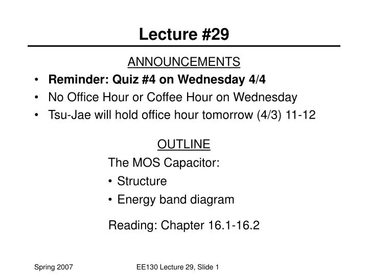
ANNOUNCEMENTS Reminder: Quiz #4 on Wednesday 4/4 No Office Hour or Coffee Hour on Wednesday Tsu-Jae will hold office hour tomorrow (4/3) 11-12 OUTLINE The MOS Capacitor: Structure Energy band diagram Reading: Chapter 16.1-16.2 Lecture #29 EE130 Lecture 29, Slide 1
MOS Capacitor Structure • Typical MOS capacitors and transistors in ICs today employ • heavily doped polycrystalline Si (“poly-Si”) film as the gate-electrode material • n+-type, for “n-channel” transistors (NMOS) • p+-type, for “p-channel” transistors (PMOS) • SiO2 as the gate dielectric • band gap = 9 eV • er,SiO2 = 3.9 • Si as the semiconductor material • p-type, for “n-channel” transistors (NMOS) • n-type, for “p-channel” transistors (PMOS) MOS capacitor (cross-sectional view) GATE xo + VG _ Si EE130 Lecture 29, Slide 2
MOS Equilibrium Energy-Band Diagram semiconductor metal oxide n+ poly-Si SiO2 EC p-type Si EC=EFM EFS EV EV EE130 Lecture 29, Slide 3
Guidelines for Drawing MOS Band Diagrams • Fermi level EF is flat (constant with distance x) in the Si • Since no current flows in the x direction, we can assume that equilibrium conditions prevail • Band bending is linear in the oxide • No charge in the oxide => dE/dx = 0 so E is constant => dEc/dx is constant • From Gauss’ Law, we know that the electric field strength in the Si at the surface, ESi, is related to the electric field strength in the oxide, Eox: E E E EE130 Lecture 29, Slide 4
MOS Band-Diagram Guidelines (cont.) • The barrier height for conduction-band electron flow from the Si into SiO2 is 3.1 eV • This is equal to the electron-affinity difference (cSi and cSiO2) • The barrier height for valence-band hole flow from the Si into SiO2 is 4.8 eV • The vertical distance between the Fermi level in the metal, EFM, and the Fermi level in the Si, EFS, is equal to the applied gate voltage: EE130 Lecture 29, Slide 5
Special Case: Equal Work Functions FM = FS EE130 Lecture 29, Slide 6
General Case: Different Work Functions E0 E0 E0 E0 EE130 Lecture 29, Slide 7
Flat-Band Condition EE130 Lecture 29, Slide 8