Download
1 / 30
540 likes | 1.21k Views
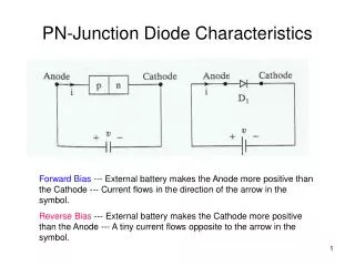
VI CHARACTERISTICS OF SEMICONDUCTOR DIODE By Prof. G. R. Agrawal. PN JUNCTIONDIODE. Biasing of PN junction diode 1. Forward bias and Reverse bias. Principle

E N D
VI CHARACTERISTICS OF SEMICONDUCTOR DIODE By Prof. G. R. Agrawal
Biasing of PN junction diode 1. Forward bias and Reverse bias
Principle • If the p-region (anode) is connected to the positive terminal of the external DC source and n-side (cathode) is connected to the negative terminal of the DC source then the biasing is said to be “forward biasing”. • Due to the negative terminal of external source connected to the n-region, free electrons from n-side are pushed towards the p-side. Similarly the positive end of the supply will push holes from p-side towards the n-side. • With increase in the external supply voltage V, more and more number of holes (p-side) and electrons (n-side) start travelling towards the junction as shown in figure. • The holes will start converting the negative ions into neutral atoms and the electrons will convert the positive ions into neutral atoms. As a result of this, the width of depletion region will reduce. • Due to reduction in the depletion region width, the barrier potential will also reduce. Eventually at a particular value of V the depletion region will collapse. Now there is absolutely no opposition to the flow of electrons and holes. • Hence a large number of electrons and holes (majority carriers) can cross the junction under the influence of externally connected DC voltage.
At the instant P-N junction formation, the free electrons near the junction in the N- region begin to diffuse across the junction in to P- region where they combine with holes near the junction. • The result is that N-region loses free electrons this creates a layer of positive charges (pentavalent ions) near the junction. • The P-region loses holes and the result that there is a negative charges (trivalent ions near the junction. • The shaded region on both sides of the junction in Fig. below contains only immobile ions and no free charge carriers such as electrons or holes. • In other words this region is depleted of free charge carriers. Therefore region is called as depletion region. • Once P-N junction is formed and depletion layer is created the diffusion of free electrons stops. • The positive and negative charges set an electric field.
i)Reverse saturation current: In reverse bias condition there will be negligible amount of current that will flow through the device due to minority carrier which is called as reverse saturation current. ii. Knee voltage: The applied forward voltage at which the PN junctions start conducting is called the cut-in voltage. It is also known as knee voltage (Vk or Vz). The value of cut-in voltage is 0.7 V for Silicon and 0.3 V for Germanium PN junction diodes. iii. Depletion layer: The region in PN junction which comprises of immobile ions is called depletion region. iv. Static resistance of diode: The resistance of a diode at the operating point can be obtained by taking the ratio of VF and IF. The resistance offered by the diode to the forward DC operating conditions is called as “DC or static resistance”.
Under reverse bias condition, the minority carrier flowing through the P- N junction acquires a kinetic energy depending upon the velocity with which they move. • The increase in reverse voltage increases the amount of kinetic energy imparted to minority carrier, as they diffuse across the PN junction. • When sufficient voltage is applied, the minority carrier acquires a large amount of kinetic energy (or momentum). • When these minority carriers collide with semiconductor (Germanium or silicon) atoms within the crystal structure of a PN junction they impart sufficient energy to break covalent bond and generate additional carrier (i.e. electron- hole pairs).
They knock out the electrons from the covalent bonds of a PN junction. • These additional carriers pick up the energy from the applied voltage and generate still more carriers. As a result of this, the reverse current through the PN junction increase. • The cumulative process of carrier generation (i.e. multiplication) is known as avalanche breakdown. • Under breakdown condition, the reverse current is no longer limited by the PN junction. But it can be limited only by the circuit components. • The value of breakdown voltage depends upon the degree of doping in PN junction.
The forward and reverse characteristics of PN junction diode
The forward characteristic is the graph of the anode to cathode forward voltage VF versus the forward current through the diode (IF). • The forward characteristics is divided into two portions, AB and BC • Region A to B of the forward characteristics. • The forward voltage is small and less than the cut in voltage. Therefore the forward current flowing through the diode is small. With further increase in the forward voltage, it reaches the level of the cut in voltage and the width the depletion region goes on decreasing
Region B to C: • As soon as the forward voltage equals the cut in voltage, current through the diode increase suddenly. The nature of this current is exponential. The large forward current in the region B-C of the forward characteristics is limited by connecting a resistor R in series with the diode. Forward current is of the order of a few mA. • The forward current is a conventional current that flows from anode to cathode. Therefore it is considered to be a positive current, and the forward characteristics appears in the first quadrant.
Cut in voltage (Knee voltage): • The voltage at which the forward diode current starts increasing rapidly is known as the cut in voltage of a diode. The cut in voltage is very close to the barrier potential. Cut in voltage is also called as knee voltage. • Generally a diode is forward biased above the cut in voltage. The cut in voltage for a silicon diode is 0.6 V and that for a germanium diode is 0.2V.
Current flowing through a diode in the reverse biased state is the reverse saturation current which flows due to the minority carriers. • Therefore it is treated as a negative current. Hence the reverse characterisitcs appears equal to Io if the temperature is constant. • As the reverse voltage is increased, the reverse saturation current remains constant equal to 10 if the temperature is constant. This is because, reverse saturation current does not depend on reverse voltage but it depends only on temperature. • But as the reverse voltage reaches the breakdown voltage value. a large current flows through the diode, due to the reasons discussed earlier. • Thus we define the reverse breakdown voltage of a pn junction diode as the reverse voltage at which breakdown takes place and a large reverse current starts flowing through the diode. • Operation in the breakdown region should be avoided because the diode may be damaged due to excessive power dissipation. • Typically the reverse breakdown voltage for p-n junction diode is in range of 50 to 100 volts.
The characteristics are similar to that of an ordinary silicon PN junction diode. • It indicates that the forward current is very small for voltages below knee voltage and large for voltages above knee (i.e. cut in) voltage. • The reverse characteristics curve indicates that negligible reverse saturation current flows until we reach the breakdown (i.e. Zener) voltage Vz • The breakdown has a very sharp knee, followed by an almost vertical increase in reverse current. • The voltage across the zener diode is approximately constant and equal to Zener voltage VZ over most of the zener breakdown region. • It will come out of the breakdown region, when the applied reverse voltage is reduced below the Zener breakdown voltage.
Working • For proper operation, the input voltage Vi must be greater than the Zener voltage Vz. This ensures that the Zener diode operates in the reverse breakdown condition. The unregulated input voltage Vi is applied to the Zener diode. • Suppose this input voltage exceeds the Zener voltage. This voltage operates the Zener diode in reverse breakdown region and maintains a constant voltage, i.e. Vz = Vo across the load inspite of input AC voltage fluctuations or load current variations. The input current is given by, IS = Vi – Vz / Rs = Vi – Vo / Rs • We know that the input current IS is the sum of Zener current Iz and load current IL. • Therefore, IS = Iz + IL or Iz = Is - IL • As the load current increase, the Zener current decreases so that the input current remains constant. According to Kirchhoff‟s voltage law, the output voltage is given by, • Vo = Vi – Is. Rs • As the input current is constant, the output voltage remains constant (i.e. unaltered or unchanged). The reverse would be true, if the load current decreases. This circuit is also correct for the changes in input voltage. • As the input voltage increases, more Zener current will flow through the Zener diode. This increases the input voltage Is, and also the voltage drop across the resistor Rs, but the load voltage Vo would remain constant. The reverse would be true, if the decrease in input voltage is not below Zener voltage.
Distinguish between PN junction diode and zener diode. PN Junction Diode Zener Diode It is properly doped to control reverse breakdown. It conducts in both directions. It is always operated in reverse-bias condition. It has quite sharp reverse breakdown. It will not burn, but functions properly in breakdown region used for voltage regulation. • It is not properly doped to control reverse breakdown. • It conducts only in one direction. • It is always operated in forward-bias condition. • It has no sharp reverse breakdown. • used for rectification
Operating Principle: • The operation of tunnel diode is based on special characteristics known as negative resistance. • The width of the depletion region is inversely proportional to the square root of impurity concentration. • So increase in the impurity concentration, the depletion region width will reduce. The thickness of depletion region of this diode is so small. That indicates there is large probability of an electron can penetrate through this barrier.
This behavior is called is tunneling & hence the name of the high impurity density PN junction is called as tunnel diode. • An ordinary PN junction diode has an impurity concentration of about 1 part in 108 and its depletion region width is of the order 5 microns. • If the concentration of impurity is increased to about 1 part in 103, the device characteristics are completely changed. Due to the thin potential energy barrier, the electrons penetrate through the junction rather than surmounting them. This quantum mechanical behavior is referred to as tunneling and these high impurity density PN junction devices are called tunnel diodes.
Application of Tunnel diode 1.In digital networks 2. High speed switch 3. High frequency oscillator
Application of Schottky diode AC to DC converter. SMPS RADAR system. Mixer and detectors in communication