
Uploaded by
pancho
1 SLIDES
123 VIEWS
10LIKES
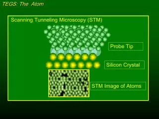
High-Resolution STM Image of Atomic Structures on Silicon Crystal Probe Tip
DESCRIPTION
This STM image captures the intricate atomic structure of silicon crystal surfaces using a Scanning Tunneling Microscope (STM). The probe tip, fashioned from sophisticated materials, allows for the visualization of individual atoms at nanometer scales. By employing advanced tunneling techniques, researchers can observe the electronic properties and arrangements of atoms, providing deep insights into material properties and behaviors. This technology is pivotal in nanotechnology and materials science, fostering advancements in electronics and nanostructures.
Download
1 / 1
Download Presentation 
High-Resolution STM Image of Atomic Structures on Silicon Crystal Probe Tip
An Image/Link below is provided (as is) to download presentation
Download Policy: Content on the Website is provided to you AS IS for your information and personal use and may not be sold / licensed / shared on other websites without getting consent from its author.
Content is provided to you AS IS for your information and personal use only.
Download presentation by click this link.
While downloading, if for some reason you are not able to download a presentation, the publisher may have deleted the file from their server.
During download, if you can't get a presentation, the file might be deleted by the publisher.
E N D
Presentation Transcript
TEGS: The Atom Scanning Tunneling Microscopy (STM) Probe Tip Silicon Crystal STM Image of Atoms


More Related