Download
1 / 19
190 likes | 208 Views
A study of SEU-tolerant latches for the RD53A chip. Denis Fougeron on behalf of the RD53 collaboration. Outline. Introduction SEU test chip description Test Set-up description Flavor of latches Hamming code version Hamming code results DICE latches versions DICE latches results

E N D
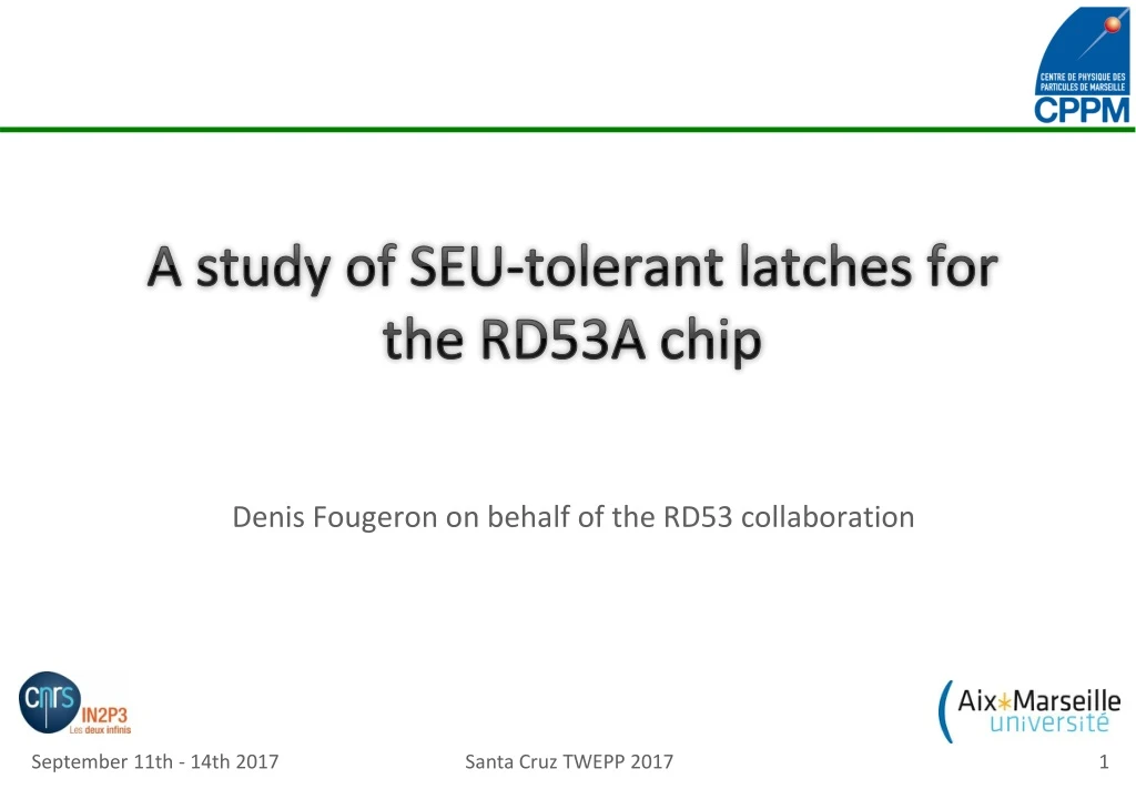
A study of SEU-tolerant latches for the RD53A chip Denis Fougeron on behalf of the RD53 collaboration Santa Cruz TWEPP 2017
Outline • Introduction • SEU test chip description • Test Set-up description • Flavor of latches • Hamming code version • Hamming code results • DICE latches versions • DICE latches results • TRL latches versions • TRL latches results • Influence of the Deep NWell • Proposal of SEU tolerant latches for the pixels of the RD53A chip • Conclusion Santa Cruz TWEPP 2017
introduction • RD53A main characteristics: • 160k pixels x 8 configuration bits=1.28M latches in totally • Technology: TSMC 65nm • TID 500 Mrad – 5 years (total fluency 1016 p/cm²) • Peak fluency ~ 0,5.109 particles/cm²/s for the layer 0 (3.7cm) • The SEU immunity for this highly scaled process should be carefully considered because the device dimensions are small and the capacitance of the storage nodes becomes very low. • Hardened By Design (HBD) approaches are used to reduce the effect of single bit upsets • 3 flavors of structure have been designed and tested • Hamming code, • Triple Redundancy Latches (TRL) cell, • Particular attention to the global nodes • Dual Interlocked CEll (DICE). • Sensitive to the charge sharing • The last SEU prototype chip allows to measure the influence of a deep N well on the digital part • Experimental test set-up • Irradiation tests were carried out at CERN using the IRRAD proton facility is located on the T8 beam-line (PS East Hall bldg 157) Santa Cruz TWEPP 2017
SEU test chip • Clmn1 • Clmn2 • Clmn3 • Clmn4 • Clmn5 • Clmn6 • Clmn7 1950µm • 3 SEU chips have been designed and allow to collect all datas from latches and directly compare their behavior during irradiation tests. • The SEU chip is sub-divided in several columns • Typically 640 cells per kind of latches • 8 Inputs, 1 output needed to monitor the chip (shown on the table above) • Custom patterns are written and read through a shift register (cf.: synoptic) in synchronization with the beam. 1950µm I/O pins of the SEU chips Example of a SEU layout 65nm chip prototype Synoptic of a SEU chip Santa Cruz TWEPP 2017
Experimental test set-up • 24 GeV protons beam line at CERN (east zone PS) • 12.1010 protons/cm²/spill • beam size 1cm² • mean dose rate • 950krad/h • TID: 500Mrad (1016p/cm²) ± 7% • exposure time 3 weeks • Mother board V2 • Collaboration with LAPP (IN2P3 ANNECY) • nanoPCBeagleBone card + FPGA • Parallel bus GPMC • Flexible programing • 40 logic signals TTL + 30 LVDS • Analog channels • 4 SAR ADC (16 bits) • 10 DAC (16 bits) • Monitoring (°C, current supply) • Lab tests + irradiation tests Dose vs time 500Mrad TID (rad) X pos. 1cm 3 weeks Y pos. X-Y Beam Profil Monitor CONTROL ROOM IRRADIATION ZONE Example of an irradiation campaign (2016) Date Time 20m length twisted pairs cable ±5V 1.2V signals Single Ended LVDS Trigger machine beam RJ45 link Intermediate board 1.2V power supply samples Mother board V2 SEU CERN setup Santa Cruz TWEPP 2017
Outline • Introduction • SEU test chip description • Test Set-up description • Flavor of latches • Hamming code version • Hamming code results • DICE latches versions • DICE latches results • TRL latches versions • TRL latches results • Influence of the Deep NWell • Proposal of SEU tolerant latches for the pixels of the RD53A chip • Conclusion Santa Cruz TWEPP 2017
Hamming code version/results • A 8 bits memory in a hamming code version has been designed with the ARTISAN library and tested during a irradiation campaign. • It needs 4 parity bits to detect and change 8 data bits. In totally, 12 bits are used for 8 configuration bits. • Main drawbacks: • A double error can’t correct the data corrupted, only a detection is possible • The dedicated area for the logic isn’t negligible but can be optimized by using the VCAD library • The results we obtained show a gain by 13 compared to a standard latch Schematic for 8 bits memory Encoder/decoder 1 bit cell Obtained results compared with a single latch Example of an area cost for a 8 bits cell in a hamming code version Santa Cruz TWEPP 2017
Outline • Introduction • SEU test chip description • Test Set-up description • Flavor of latches • Hamming code version • Hamming code results • DICE latches versions • DICE latches results • TRL latches versions • TRL latches results • Influence of the Deep NWell • Proposal of SEU tolerant latches for the pixels of the RD53A chip • Conclusion Santa Cruz TWEPP 2017
DICE versions • DICE latch structure is based on the conventional cross coupled inverters: • The charges deposited by a ionising particle strike one node can’t be propagated due to the stability of this architecture. • If 2 sensitive nodes (corresponding to the OFF transistors drain area) are affected simultaneously, the immunity is lost and the DICE latch is upset • In this case, the equivalent critical charge becomes very low • Spatial distance between 2 sensitive pair nodes (D2N) must be increased • 4 versions have been submitted: OFF ON ON OFF 1 0 1 0 ON ON OFF OFF Sensitive pair nodes DICE schematic (example of a stored data = 1) 3.5µm 6µm • Version 1 • DICE structure • WPMOS/LPMOS=400nm/60nm • WNMOS/LNMOS=200nm/60nm • D2N = 1.2µm • Version 2 • Version 1 + guard rings • D2N = 2µm 2µm 1.2µm 2µm 2µm Layout DICE version 1 Layout DICE version 2 • Version 4 • ↑ the size of transistors • ↑the node capacitance • WPMOS/LPMOS=400/400nm • WNMOS/LNMOS=200/400nm • D2N = 2µm • Interleaved version has been tested 7µm 5.6µm • Version 3 • Version 1 interleaved • D2N ↑up to 12µm bit 1 bit 2 12µm 2µm 2µm 2µm 12µm Layout DICE version 4 Layout DICE version 3 Santa Cruz TWEPP 2017
DICE latches results reminder of DICE version Synthesis of DICE results • We stored enough data to extract an acceptable statistic for SEU • 640 cells per type of latch and we reached a spill number > 20000 • Cross section of the standard latch ~ 2.8E-14 cm² • Dice latch is ~ 5 x immune to SEU than standard latch • With interleaved layout, improvement of the SEU tolerance : 9 x more tolerant than the standard latch -> cross section = 3.1E-15cm² • By increasing the size of transistors (L X 7), we win a gain value significantly (~30) while keeping an area budget compatible with the pixel size (50x50um). Santa Cruz TWEPP 2017
Outline • Introduction • SEU test chip description • Test Set-up description • Flavor of latches • Hamming code version • Hamming code results • DICE latches versions • DICE latches results • TRL latches versions • TRL latches results • Influence of the Deep NWell • Proposal of SEU tolerant latches for the pixels of the RD53A chip • Conclusion Santa Cruz TWEPP 2017
TRL versions bit 1 bit 2 • 3 TRL versions have been designed and tested at CERN • Reference version with a feedback correction commanded by a latch error detection • 2nd version with an insertion of a delay cell (5ns ± 1ns) on the LOAD common node • 3rd version: triplication of the LOAD function with a special attention of the associated layout and a respect of a minimum distance between 2 bits (~17µm) 2nd TRL version 3rd TRL version reference TRL version 38µm Bit2 17µm 4µm Bit1 Layout of the 3rd TRL version (2 bits) Santa Cruz TWEPP 2017
TRL latches results Synthesis of TRL results reminder of TRL version • Enough statistics for SEU (640 cells per flavor of cell and > 20 000 spills) • Cross section standard latch ~ 2.8E-14 cm² • TRL latch is ~200 x immune to SEU than standard latch (same result as for the PROTO65_V1) • Triplication of the “load path” improves the SEU tolerance by a factor 5 ( ~1000 x times immune than a standard latch) • Cross section ~ 2.3 E-17 cm² • With interleaved layout added the load signal triplication, SEU tolerance improved by a factor 18 regarding the reference TRL design (version 1). It represents an immunity 4E3 better than the standard latch • Cross section ~ 6.8 E-18 cm² Santa Cruz TWEPP 2017
Outline • Introduction • SEU test chip description • Test Set-up description • Flavor of latches • Hamming code version • Hamming code results • DICE latches versions • DICE latches results • TRL latches versions • TRL latches results • Influence of the Deep NWell • Proposal of SEU tolerant latches for the pixels of the RD53A chip • Conclusion Santa Cruz TWEPP 2017
Influence of the DNW • DNW is used to optimize an isolation between a sensitive part and the digital functions associated. This option is implemented in the RD53A chip. • Some perturbations in term of SEU rate due to the presence of parasitic bipolar transistors. • Direct comparison between 2 cells with and without DNW is possible with our last SEU prototype. • No real difference measured between these 2 cells • A DNW in this technology doesn’t affect the SEU tolerance Layout of 2 cells with (left) and without (right) DNW Synthesis error rate/spill N+ N+ N+ P+ P+ P+ N+ N+ NW NW PW NW DNW PSUB CMOS with a Deep N Well Cross section SR vs SR_DNW Santa Cruz TWEPP 2017
Outline • Introduction • SEU test chip description • Test Set-up description • Flavor of latches • Hamming code version • Hamming code results • DICE latches versions • DICE latches results • TRL latches versions • TRL latches results • Influence of the Deep NWell • Proposal of SEU tolerant latches for the pixels of the RD53A chip • Conclusion Santa Cruz TWEPP 2017
Proposal of SEU latches for RD53A • A configuration memory pixel has been designed and implemented in few columns in the RD53A chip submitted at the end of august. • It is equivalent to the DICE version 3 cell: • Interleaved version • Transistors size PMOS: 400nm/60nm, NMOS: 200nm/60nm • Distance between 2 DICE’s (D2N) ~10µm Area of this block Synoptic of the block memory Layout of the block memory Santa Cruz TWEPP 2017
conclusion • Several flavor of latches have been tested to evaluate their tolerance against the SEU effect • Triple Redundancy Latches versus DICE retain our attention during this study • TRL: • very tolerant to the SEU (Cross section ~ 6.8 E-18 cm²) • Compatible in a periphery of a full scale chip (global memory) • DICE: • Dedicated area compatible implementation in a pixel but sensitive to the charge sharing • Optimization of the size transistors is a good issue without affecting a lot the cost of area • The hamming code version could be improve: • Only a factor 13 comparing with a standard latch • Parity bit architecture more tolerant, optimization of the area ratio logic/latches, … • The implementation of a Deep Nwell to isolate the digital part doesn’t show a degradation of the SEU cross section • The parasitic bipolar presents with the DNW layerdoesn’t affect the cross section of the memory • RD53A side: • A pixel configuration 8 bits memory has been designed and implemented in the chip • A TRL architecture has been synthetized and implemented in the periphery Mean time errors estimation relative to cross section measured Santa Cruz TWEPP 2017
THANKS FOR YOUR ATTENTION Santa Cruz TWEPP 2017