
CS 6560 Operating System Design
E N D
Presentation Transcript
CS 6560 Operating System Design Lecture 8: Memory Management
References • Our textbook: Robert Love, Linux Kernel Development, 2nd edition, Novell Press, 2005. • Understanding the LINUX Kernel, 3rd. edition, O’Reilly, 2005. (covers 2.6) • The kernel code and its own documentation. • Also see Ulrich Drepper’sarticles in LWN.net • Part I: http://lwn.net/Articles/250967/ • Part II: http://lwn.net/Articles/252125/ • Part III: http://lwn.net/Articles/253361/
Plan • Preliminaries Today • Next time: Chap 11: Memory Management
Models of Memory • Models of Memory • Physical: RAM array accessed through a memory controller • Real: Linear array of bytes for entire machine • Virtual: Linear array of bytes for each process.
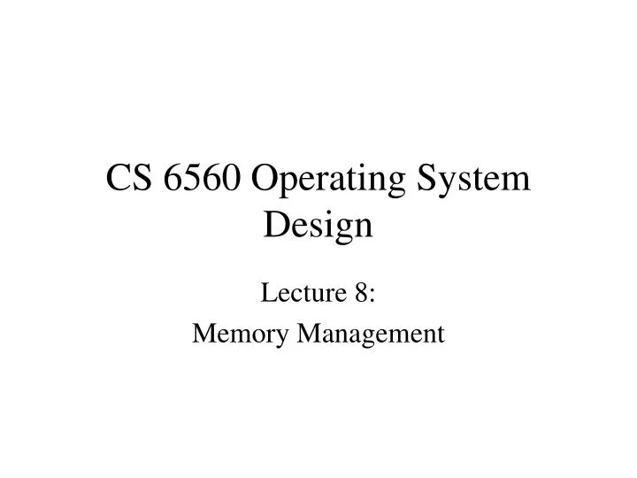
Physical Model Memory Array Memory Controller Bus
Physical Model of Memory • Physical Models (See Drepper’s article for details) • Bits in SRAM and DRAM • SRAM = static RAM - faster, but several transistors per bit • DRAM - dynamic RAM - slower, each bit requires only one transistor, but needs refreshing • Many types of DRAM with differing speeds of memory array and bus
Physical Memory Issues • Accessing main memory may be slow: • Large addressing requires multiplexing which slows access. • DRAM refresh requires time. • DRAM speed is limited by power consumption considerations. • The speed of light limits access time. c = 299,792,458 meters/second = .299792458 meters/nanosecond. That’s about 10 cm for one cycle of a 3Gig clock • Other considerations • A serial bus can run much faster than a parallel bus. • Parallel busses cost more and use more space. • The memory itself may run slower than the bus (DDR2).
CPU/Memory • Various arrangements: • CPUs, memory, and peripherals share the same bus (classical IBM PC). • CPUs and memory share the same bus (FSB), but peripherals share another bus (PCI bus). • Each CPU has its own memory (AMD Opteron and Intel CSI). Then CPUs share a bus or form a network that connects to the bus.
DMA • DMA = Direct Memory Access • Here, the CPU sets up a data transfer between memory and a device, but does not participate in the actual transfer. A DMA controller does the transfer on behalf of the processor.
Processor Hierarchy • Processors, Cores, and Threads: • Cores - run programs simultaneously with own instruction processing units, but share chip infrastructure. • Threads (hyperthreading) - run programs in interleaving fashion with separate register sets. • Modern CPUs are designed for multiplicity at all levels (say 2 threads/core, 4 cores/processor, 2 processors/motherboard)
Challenges • CPUs are getting significantly faster than main memory. • CPUs are evolving to multiple parallel processing units. • Main memory is being distributed among processing units (NUMA)
Memory Caching • Caching schemes • Cache memory sits in between CPU and main memory. • Different levels and arrangements of cache • Main memory tends to consist of DRAM and caches tend to consist of SRAM.
Various levels of memory • Registers: typical size 512 = 2^9 - typical access time 1 cycle • L1: typical size 64KB = 2^16 - typical access time 3 cycles • L2: typical size 4MB = 2^22 - typical access time 14 cycles • Main memory: typical size 2GB = 2^31 - typical access time 240 cycles Note: sizes are for Intel IA-32 Core technology (see sandpile.org)
How to Caches Work? • Cache is divided into what are called cache lines. Each cache line has several bytes of data (64 bytes of data per line for Intel Core) plus addressing information (say 32 bits). (The cache size is computed just from the data size.) • The cache lines are divided into sets (say 8192 sets, with 8 lines per set ) (say, 2^13 * 2^3 * 2^6 = 2^22 = 4MB). • Cache addressing information is split into fields (say T, S and O). • The rightmost field O is used for addressing within the cache lines (say 6 bits for 64 byte cache lines). • The middle field S is used determine which set (say 13 bits) • The left field T (say 13 bits) is used for matching the address.
Associativity • The address matching is done with a comparator. • The number of items that can be compared is called the associativity. • Modern processors typically achieve 2-way, 8-way or 16-way associativity.
Cashe Hits and Misses • Caching works in levels. With three levels • If the data cannot be matched in the L1 cache, then the L2 cache is checked. • If the data cannot be found at L2, L3 is checked. • If not in L3, get it from main memory.
Cache Sharing and Snooping • Often cores will have their own L1 caches, one for data and one for instructions, and a shared L2 cache that contains both data and instructions. • When two or more processing units share memory or the next level cache, they may snoop on each other’s individual cache and exchange data if needed. • Popular cache snooping algorithms include MESI and SI. In these, the address bus is available from each processing to the other and a finite state machine determines fate of a cache line according to whether it was locally or remotely read or written to.
MESI • MESI has four states for each cache line • M = Modified = modified by local processing unit and only copy • E = Exclusive = only copy, but not modified • S = Shared = not modified, and might be shared • I = Invalid = unused or invalid
Transition Table • Each local or remote read or write changes the state according to something like: *Also transmits data to other processor and to memory +Also notifies other processors with RFO
80x86 Processor Memory • Memory addressing modes • Logical Address: segment, offset pair • Linear Address: virtual memory address • Physical address: hardware - 32 bit or 36-bit number
Memory addressing modes • Real: logical to physical mapping uses formula 16*seg + offset • Protected: uses MMU to map from logical to physical by way of linear.
MMU • MMU (Protected Mode) maps in two stages • Segmentation Unit: uses Segment Descriptors to map logical to linear addresses • Paging Unit: Uses Page Table to map linear addresses to physical addresses
Segment Descriptor Tables • Two types • GDT = Global Descriptor Table • LDT = Local Descriptor Table • Linux mainly uses the GDT (at least in the kernel memory). The LDT may be used to help emulate other OSs in user mode. • Types of descriptors (8 bytes) • Code • Data • Task State • Local
Fields of Segment Descriptors • Fields (distributed within descriptor) • Base (32-bits) = linear address of first byte of segment • G (1-bit) = granularity of segment size (bytes or 4K) • Limit (20-bits) = size of segment (two cases of G) • S (1-bit) = System flag (1=system data) • Type (4-bits) • DPL (2-bits) = descriptor privilege • P (1-bit) segment present (Linux has this as 1)
Segment Selectors • Segment info is stored in 16-bit segment selector, contains • Index: index into the GDT or LDT • TI: choice of which table, 0=GDT, 1=LDT • Privilege level • Six segment registers in the CPU • cs, ss, ds, es, fs, gs • First three are special purpose: code, stack, data • cs also contains privilege level (0=kernel, 3=user)
Segmentation in Linux • Very limited - only when required by processor. • All user process use the same code and data segment descriptors. • The kernel has a separate code and data segment descriptors.
Linux GDT • Each CPU has its own GDT. These are stored in cpu_gdt_decr array. • Each GDT has 18 segment descriptors for • Four user/kernel code/data • A Task State Segment (TSS) to help switch between user and kernel mode and when users access I/O ports • A segment containing the LDT • Three Thread-Local Storage segments • Three Power Management segments • Five Plug and Play segments • One special TSS for exception handling
Virtual Memory • Virtual Memory in Linux divides memory into pages which are either 4K or 4M. (The i386 uses segmentation as well.) (on 64-bit architecture, pages may be 8K) • The Memory Management Unit (MMU) maps virtual addresses (linear) to physical addresses. • The kernel fills in the page mapping table (called the page directory), but the MMU hardware does the work. • The page table contains other information about each page including permission. • On a 32-bit virtual addressing space, the kernel sees both the process user addressing space and the kernel addressing space. The kernel appears in the upper 1G and the user space as the lower 3G.
Page Faults • If a page is not in memory, a page fault interrupt is generated. • Code for handling the fault (for i386) is in ./arch/i386/mm • Page faults should not happen in the kernel. How this is arranged is explained in chap 11 (coming up soon).
Two types of 32-bit paging • Regular - pages 4KB • Extended (Pentium) - pages 4MB
Linear Address Fields • For 32-bit regular paging (4KB), the linear address consist of three bit fields • Directory (bits 22-31) (10 bits) • Table (bits 12-21)(10 bits) • Offset (bits 0-11)(12 bits) • For 32-bit extended (4MB) • Directory (bits 22-31) (10 bits) • Offset (bits 0-21) (22 bits) • For 64-bit, there are more (later).