Download
1 / 19
190 likes | 363 Views
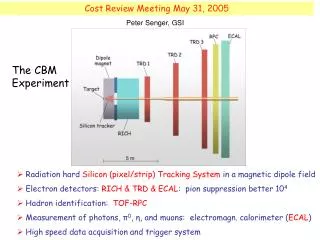
Development of radiation hard microstrip detectors for the CBM Experiment. Sudeep Chatterji GSI Helmholtz Centre for Heavy Ion Research CBM Collaboration Meeting 12 April, 2010. CBM Silicon Tracking System Layout. Fluka Simulation. 1m.

E N D
Development of radiation hard microstrip detectors for the CBM Experiment Sudeep Chatterji GSI Helmholtz Centre for Heavy Ion Research CBM Collaboration Meeting 12 April, 2010
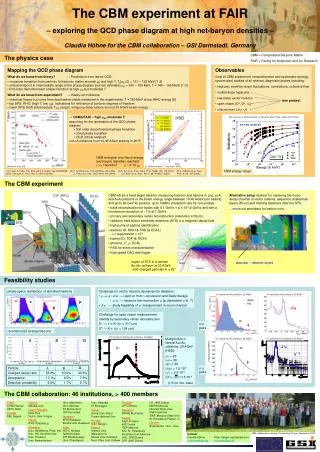
CBM Silicon Tracking System Layout Fluka Simulation 1m • STS has 8 stations of DSSDs, Strip Pitch ~ 58 mm, Strip Width ~ 20 mm, stereo angle ~ 7.5 0 • Expected Radiation Damage ~ 1 x 10¹⁴ neq cm-2 year-1 • Need detailed simulations to optimize device parameters to maximize VBD and minimize Noise. • Also simulation needed to understand the impact of radiation damage.
3-Dimensional Grid • 3-D TCAD simulation tools “SYNOPSYS” • Sub packages • Sentaurus • Inspect • Tecplot • SPICE (Mixed Mode) x set by strip pitch y set by stereo angle
Stereo Angle in Strips X-Y plane of the 3D grid. One can see there is a stereo angle on either side of 7.50.
Implementing Bias Ring & Resistor • System { • Strip sample (nplus1=c1 nplus2=c2 nplus3=c3 nplus4=c4 pplus1=cp1 pplus2=cp2 pplus3=cp3 pplus4=cp4) • Vsource_pset vn (dd 0) {dc=0} • Vsource_pset vp (dd1 0) {dc=0} • Resistor_pset rn1 (c1 dd) {resistance=2000000} • Resistor_pset rn2 (c3 dd) {resistance=2000000} • Resistor_pset rp1 (cp1 dd1) {resistance=2000000} • Resistor_pset rp2 (cp3 dd) {resistance=2000000} • } • Solve { • Circuit • Coupled (Iterations=100) {Poisson} • Coupled {Poisson Electron Hole Contact Circuit} • Quasistationary ( • InitialStep=1e-3 MaxStep=0.025 Minstep=3e-5 Increment=1.2 • Goal { Parameter = vp.dc Voltage = -100} • Goal {Parameter = vn.dc Voltage=0} • ) • } • Implementing Pulse Generator (Future Plan) • Vsource_pset vin (node1 node2) {pulse=(DCStart Vamptd trtftperiod)} • Can simulate the entire readout chain Mixed Mode Simulation (PSpice in TCAD)
Understanding the Geometry • Using SYNOPSYS TCAD 3-D simulation package • Silicon volume ~ Cuboid (Six Rectangular faces). • Dopant Implants, P-Stop and Contacts ~ Parallelogram • Oxide ~ Cuboid, Enough space needed at the corners for junction curvature (0.8*Junction Depth)
Some Static Characteristics • CTotal = Cback+2*Cint • ENC αCTotal • Optimization needed to maximize breakdown voltage & minimize ENC
Optimization of W/P & P-Spray Width • When W/P is too small, there is inappreciable impact of ↑ the strip width on VBD • A narrower strip width and a wide P-Spray width can reduce the ENC.
Optimization of P-Spray Dose Mixed Mode Simulation (TCAD + SPICE) • With ↑ in P-Spray dose, the VBD ↓ • Using P-Spray rather than P-Stop seems better for detector performance • What happens at high radiation damage?
Radiation Damage in Silicon • The major effect expected from bulk damage is the change in the effective • carrier concentration (Neff) leading to Type Inversion. • The change in Neff is parameterized using Hamburg model: • The change in Minority carrier lifetime is parameterized using Kraners model: • For high quality oxide, the value of surface oxide charge (Qf) is expected to be • 3e11cm-2 (for non-irradiated detector) while after irradiation Qf increases and • saturates at about 1e12 cm-2. Flatband Voltage gives an approx. of Qf.
Type Energy (eV) Trap σe (cm2) σh (cm2) η (cm-1) Acceptor Ec-0.42 VV 2.0*10-15 2.0*10-14 1.613 Acceptor Ec-0.46 VVV 5.0*10-15 5.0*10-14 0.9 Donor Ev+0.36 CiOi 2.5*10-14 2.5*10-15 0.9 Impact of Radiation Damage • VBD↑ with fluence • Current ↑ by 3 orders • Rint ↓ with fluence • Detailed study needed Trap Model, University of Perugia
Transient Simulations • Can simulate the passage of Heavy Ion, α-particle and Laser. • Can include angle in the passage of MIPs. • Plan to do complete scan of interstrip region and compare with test beam data.
Simulation of Readout Cables • Two connecting layers with constant pitch of 100 mm are laminated together with a lateral shift of 50 mm. • A spacer layer is inserted between the two layers to reduce the capacitance. • An external shielding layer is applied to reduce the noise.
Simulation of Readout Cables 3-D grid of the kapton cable 3-D grid without insulator
Summary • We need radiation hard Double Sided Silicon Strip detectors. • TCAD simulation package, SYNOPSYS has been installed on • CBM batch farm and running. • We are doing Mixed Mode simulation using SPICE models • available in Sentaurus. • Have procured the Probe Station. • Plan to carry out measurements before and after irradiation both • with proton and with neutrons. • Carry out systematic annealing studies. • Work closely with CiS, Erfurt on microstrip detector R&D.