Download
1 / 2
20 likes | 39 Views
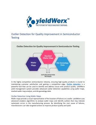
Outlier detection is a powerful tool that can be used to identify and address issues with product quality. yieldWerx yield management system provides advanced outlier detection capabilities using wafer maps, stacked wafer map analysis, and die genealogy data.

E N D
Outlier Outlier Detection Detection for Testing Testing for Quality Quality Improvement Improvement in in Semiconductor Semiconductor In the highly competitive semiconductor industry, ensuring high-quality products is crucial to maintaining customer satisfaction and gaining a competitive edge. Outlier detection is a powerful tool that can be used to identify and address issues with product quality. yieldWerx yield management system provides advanced outlier detection capabilities using wafer maps, stacked wafer map analysis, and die genealogy data. Outlier Detection Using Wafer Maps Outlier Detection Using Wafer Maps Wafer maps provide a visual representation of the location of failures on a wafer. yieldWerx uses advanced analytics algorithms to analyze wafer maps and identify outliers that may indicate systematic errors in the manufacturing process. By identifying the root cause of failures, manufacturers can take targeted actions to improve product quality and yield.
Stacked Wafer Map Analysis Stacked Wafer Map Analysis Stacked wafer map analysis is a technique used to identify hotspots and patterns of failing die across multiple wafers. This method involves aligning multiple wafer maps and stacking them on top of each other to identify common patterns or clusters of failing die. yieldWerx uses advanced algorithms to identify the causes of hotspots and patterns of failures and provides valuable insights into the semiconductor manufacturing process. Die Genealogy Data Die Genealogy Data Die genealogy data includes information about pass and fail outcomes, parametric data, and wafer and lot identification. yieldWerx uses die genealogy data to trace the genealogy of each die and identify any patterns or trends that may indicate issues with the manufacturing process. By analyzing die genealogy data, manufacturers can gain valuable insights into the causes of failures and take appropriate actions to address them. In conclusion, outlier detection using wafer maps, stacked wafer map analysis, and die genealogy data is an essential tool for semiconductor manufacturers to improve quality and yield. yieldWerx provides advanced analytics and visualization tools to help manufacturers identify and address issues with product quality. By using yieldWerx, manufacturers can gain valuable insights into the manufacturing process and take precise actions to improve product quality and yield. Add Ons Add Ons Automated Assemble Map Generation Cross Work Center Correlation Quality Assurance & Risk Elimination External Data Source Integration Real time Lot Control and Disposition Executive Dashboard Smart Wafer Merge Automated Data Loading Raw Data Monitoring Yield Calculation Flexibility SPC/SBL/SYL Production Yield Reporting Standard Data Access Lot Genealogy Part Average Testing 15 Day Free Trial Schedule a Demo