Download
1 / 80
860 likes | 1.09k Views
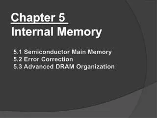
Chapter 5. The Memory System. Overview. Basic memory circuits Organization of the main memory Cache memory concept Virtual memory mechanism Secondary storage. Some Basic Concepts. Basic Concepts.

E N D
Overview • Basic memory circuits • Organization of the main memory • Cache memory concept • Virtual memory mechanism • Secondary storage
Basic Concepts • The maximum size of the memory that can be used in any computer is determined by the addressing scheme. 16-bit addresses = 216 = 64K memory locations • Most modern computers are byte addressable. W ord address Byte address Byte address 0 0 1 2 3 0 3 2 1 0 4 4 5 6 7 4 7 6 5 4 • • • • • • k k k k k k k k k k 2 - 4 2 - 4 2 - 3 2 - 2 2 - 1 2 - 4 2 - 1 2 - 2 2 - 3 2 - 4 (a) Big-endian assignment (b) Little-endian assignment
Traditional Architecture Memory Processor k -bit address bus MAR n -bit data bus k Up to 2 addressable MDR locations Word length = n bits Control lines R / W ( , MFC, etc.) Figure 5.1.Connection of the memory to the processor.
Basic Concepts • “Block transfer” – bulk data transfer • Memory access time • Memory cycle time • RAM – any location can be accessed for a Read or Write operation in some fixed amount of time that is independent of the location’s address. • Cache memory • Virtual memory, memory management unit
Internal Organization of Memory Chips b b ¢ b b ¢ b b ¢ 7 7 1 1 0 0 • • • W 0 FF FF A • • • 0 W 1 A 1 Address Memory • • • • • • • • • • • • • • • • • • cells decoder A 2 A 3 • • • W 15 16 words of 8 bits each: 16x8 memory org.. It has 16 external connections: addr. 4, data 8, control: 2, power/ground: 2 1K memory cells: 128x8 memory, external connections: ? 19(7+8+2+2) 1Kx1:? 15 (10+1+2+2) R / W Sense / Write Sense / Write Sense / Write circuit circuit circuit CS Data input /output lines: b b b 7 1 0 Figure 5.2.Organization of bit cells in a memory chip.
A Memory Chip 5-bit row address W 0 W 1 32 ´ 32 5-bit memory cell decoder array W 31 Sense / Write circuitry 10-bit address 32-to-1 R / W output multiplexer and CS input demultiplexer 5-bit column address Data input/output Figure 5.3. Organization of a 1K 1 memory chip.
Static Memories • The circuits are capable of retaining their state as long as power is applied. b b ¢ T T 1 2 X Y Word line Bit lines Figure 5.4. A static RAM cell.
Static Memories • CMOS cell: low power consumption
Asynchronous DRAMs • Static RAMs are fast, but they cost more area and are more expensive. • Dynamic RAMs (DRAMs) are cheap and area efficient, but they can not retain their state indefinitely – need to be periodically refreshed. Bit line Word line T C Figure 5.6.A single-transistor dynamic memory cell
A Dynamic Memory Chip R A S Row Addr. Strobe Row Row 4096 ´ ( 512 ´ 8 ) address decoder cell array latch A ¤ A CS Sense / Write 20 - 9 8 - 0 circuits R / W Column Column address decoder latch C A S D D 7 0 Column Addr. Strobe Figure 5.7. Internal organization of a 2M ´ 8 dynamic memory chip.
Fast Page Mode • When the DRAM in last slide is accessed, the contents of all 4096 cells in the selected row are sensed, but only 8 bits are placed on the data lines D7-0, as selected by A8-0. • Fast page mode – make it possible to access the other bytes in the same row without having to reselect the row. • A latch is added at the output of the sense amplifier in each column. • Good for bulk transfer.
Synchronous DRAMs • The operations of SDRAM are controlled by a clock signal. Refresh counter Row Ro w address Cell array decoder latch Row/Column address Column Co lumn Read/Write address circuits & latches decoder counter Clock R A S Mode register Data input Data output C A S and register register timing control R / W C S Data Figure 5.8.Synchronous DRAM.
Synchronous DRAMs Clock R / W R A S C A S Address Row Col Data D0 D1 D2 D3 Figure 5.9.Burst read of length 4 in an SDRAM.
Synchronous DRAMs • No CAS pulses is needed in burst operation. • Refresh circuits are included (every 64ms). • Clock frequency > 100 MHz • Intel PC100 and PC133
Latency and Bandwidth • The speed and efficiency of data transfers among memory, processor, and disk have a large impact on the performance of a computer system. • Memory latency – the amount of time it takes to transfer a word of data to or from the memory. • Memory bandwidth – the number of bits or bytes that can be transferred in one second. It is used to measure how much time is needed to transfer an entire block of data. • Bandwidth is not determined solely by memory. It is the product of the rate at which data are transferred (and accessed) and the width of the data bus.
DDR SDRAM • Double-Data-Rate SDRAM • Standard SDRAM performs all actions on the rising edge of the clock signal. • DDR SDRAM accesses the cell array in the same way, but transfers the data on both edges of the clock. • The cell array is organized in two banks. Each can be accessed separately. • DDR SDRAMs and standard SDRAMs are most efficiently used in applications where block transfers are prevalent.
Structures of Larger Memories 21-bit addresses 19-bit internal chip address A 0 A 1 A 19 A 20 2-bit decoder 512 K ´ 8 memory chip D D D D 31-24 23-16 15-8 7-0 512 K ´ 8 memory chip 19-bit 8-bit data address input/output Chip select Figure 5.10. Organization of a 2M 32 memory module using 512K 8 static memory chips.
Memory System Considerations • The choice of a RAM chip for a given application depends on several factors: Cost, speed, power, size… • SRAMs are faster, more expensive, smaller. • DRAMs are slower, cheaper, larger. • Which one for cache and main memory, respectively? • Refresh overhead – suppose a SDRAM whose cells are in 8K rows; 4 clock cycles are needed to access each row; then it takes 8192×4=32,768 cycles to refresh all rows; if the clock rate is 133 MHz, then it takes 32,768/(133×10-6)=246×10-6 seconds; suppose the typical refreshing period is 64 ms, then the refresh overhead is 0.246/64=0.0038<0.4% of the total time available for accessing the memory.
Memory Controller Row/Column address Address R A S R / W C A S Memory controller Request R / W Processor Memory C S Clock Clock Data Figure 5.11. Use of a memory controller.
Not connected to store a 1 Connected to store a 0 Read-Only-Memory • Volatile / non-volatile memory • ROM • PROM: programmable ROM • EPROM: erasable, reprogrammable ROM • EEPROM: can be programmed and erased electrically Bit line Word line T P Figure 5.12.A ROM cell.
Flash Memory • Similar to EEPROM • Difference: only possible to write an entire block of cells instead of a single cell • Low power • Use in portable equipment • Implementation of such modules • Flash cards • Flash drives
Speed, Size, and Cost Pr ocessor Re gisters Increasing Increasing Increasing size speed cost per bit Primary L1 cache Secondary L2 cache Main memory Magnetic disk secondary memory Figure 5.13.Memory hierarchy.
Cache • What is cache? • Why we need it? • Locality of reference (very important) - temporal - spatial • Cache block – cache line • A set of contiguous address locations of some size Page 315
Cache • Replacement algorithm • Hit / miss • Write-through / Write-back • Load through Main Processor Cache memory Figure 5.14.Use of a cache memory.
Memory Hierarchy I/O Processor Main Memory CPU Cache Magnetic Disks Magnetic Tapes
Cache Memory • High speed (towards CPU speed) • Small size (power & cost) MainMemory (Slow)Mem Miss CPU Cache(Fast)Cache Hit 95% hit ratio Access = 0.95 Cache + 0.05 Mem
Cache Memory MainMemory 1 Gword CPU 30-bit Address Cache1 Mword Only 20 bits !!!
Cache Memory MainMemory 00000000 00000001 • • • • • • • • • • 3FFFFFFF Cache 00000 00001 • • • • FFFFF Address Mapping !!!
Direct Mapping Main memory Block 0 Block 1 Block j of main memory maps onto block j modulo 128 of the cache Block 127 Cache tag Block 0 Block 128 tag Block 1 Block 129 4: one of 16 words. (each block has 16=24 words) 7: points to a particular block in the cache (128=27) 5: 5 tag bits are compared with the tag bits associated with its location in the cache. Identify which of the 32 blocks that are resident in the cache (4096/128). tag Block 127 Block 255 Block 256 Block 257 Figure 5.15.Direct-mapped cache. Block 4095 T ag Block W ord 5 7 4 Main memory address
Direct Mapping Address What happens when Address= 100 00500 000 00500 Cache 00000 000 0 1 A 6 00500 Tag Data 4 7 C C 000 0 1 A 6 00900 080 0 0 0 5 01400 150 FFFFF Compare Match No match 20Bits(Addr) 10 Bits(Tag) 16 Bits(Data)
Direct Mapping with Blocks Address 000 0050 0 Block Size = 16 Cache 00000 000 0 1 A 60 2 5 4 0050000501• Tag Data 4 7 C CA 0 B 4 000 0 1 A 6 0090000901• 080 0 0 0 55 C 0 4 150 0140001401• FFFFF Compare Match No match 20Bits(Addr) 10 Bits(Tag) 16 Bits(Data)
Direct Mapping • Tag: 11101 • Block: 1111111=127, in the 127th block of the cache • Word:1100=12, the 12th word of the 127th block in the cache T ag Block W ord 5 7 4 Main memory address 11101,1111111,1100
Associative Mapping Main memory Block 0 Block 1 Cache tag Block 0 tag Block 1 Block i tag Block 127 4: one of 16 words. (each block has 16=24 words) 12: 12 tag bits Identify which of the 4096 blocks that are resident in the cache 4096=212. Block 4095 T ag W ord Main memory address 12 4 Figure 5.16. Associative-mapped cache.
Associative Memory Cache Location MainMemory 00000000 00000001 • • 00012000 • • 08000000 • • 15000000 • 3FFFFFFF Cache 00000 00001 • • • • FFFFF 00012000 15000000 08000000 Address (Key) Data
Associative Mapping Address 00012000 Cache Can have any number of locations 00012000 0 1 A 6 Data 0 0 0 5 15000000 0 1 A 6 4 7 C C 08000000 How many comparators? 30 Bits(Key) 16 Bits(Data)
Associative Mapping • Tag: 111011111111 • Word:1100=12, the 12th word of a block in the cache T ag W ord Main memory address 12 4 111011111111,1100
Set-Associative Mapping Main memory Block 0 Block 1 Cache tag Block 0 Set 0 Block 63 tag Block 1 Block 64 tag Block 2 Set 1 Block 65 tag Block 3 4: one of 16 words. (each block has 16=24 words) 6: points to a particular set in the cache (128/2=64=26) 6: 6 tag bits is used to check if the desired block is present (4096/64=26). Block 127 tag Block 126 Set 63 Block 128 tag Block 127 Block 129 Block 4095 Figure 5.17. Set-associative-mapped cache with two blocks per set. T ag Set W ord 6 6 4 Main memory address
Set-Associative Mapping Address 000 00500 2-Way Set Associative Cache 00000 000 0 1 A 6 00500 010 0 7 2 1 Tag2 Data2 Tag1 Data1 010 0 7 2 1 4 7 C C 000 0 1 A 6 00900 080 0 8 2 2 000 0 0 0 5 01400 150 0 9 0 9 000 FFFFF Compare Compare 20Bits(Addr) 10 Bits(Tag) 16 Bits(Data) 10 Bits(Tag) 16 Bits(Data) Match No match
Set-Associative Mapping • Tag: 111011 • Set: 111111=63, in the 63th set of the cache • Word:1100=12, the 12th word of the 63th set in the cache T ag Set W ord 6 6 4 Main memory address 111011,111111,1100
Replacement Algorithms • Difficult to determine which blocks to kick out • Least Recently Used (LRU) block • The cache controller tracks references to all blocks as computation proceeds. • Increase / clear track counters when a hit/miss occurs
Replacement Algorithms • For Associative & Set-Associative Cache Which location should be emptied when the cache is full and a miss occurs? • First In First Out (FIFO) • Least Recently Used (LRU) • Distinguish an Empty location from a Full one • Valid Bit
Replacement Algorithms CPU Reference A B C A D E A D C F Miss Miss Miss Hit Miss Miss Miss Hit Hit Miss A A A A A E E E E E Cache FIFO B B B B B A A A A C C C C C C C F D D D D D D Hit Ratio = 3 / 10 =0.3
Replacement Algorithms CPU Reference A B C A D E A D C F Miss Miss Miss Hit Miss Miss Hit Hit Hit Miss A B C A D E A D C F Cache LRU A B C A D E A D C A B C A D E A D B C C C E A Hit Ratio = 4 / 10 =0.4
Overview • Two key factors: performance and cost • Price/performance ratio • Performance depends on how fast machine instructions can be brought into the processor for execution and how fast they can be executed. • For memory hierarchy, it is beneficial if transfers to and from the faster units can be done at a rate equal to that of the faster unit. • This is not possible if both the slow and the fast units are accessed in the same manner. • However, it can be achieved when parallelism is used in the organizations of the slower unit.