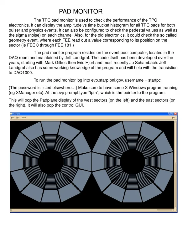
ABCN Pad ring
ABCN Pad ring. V 7.0. Revised for power names, io cell name, pads order and pad positions. To BE. To FE. ABC130 “RIGHT SIDE”. Chip edge. REG_D fake. REG_A fake. ShuntCtrl. L0_COM. LVDS R. LVDS R. LVDS R. LVDS R. R3_L1. RLCK. BC. SIOGND. SIOGND. CMOS. SIOGND. SIOGND.


ABCN Pad ring
E N D
Presentation Transcript
ABCN Pad ring V7.0 Revised for power names, io cell name, pads order and pad positions F. Anghinolfi
To BE To FE ABC130 “RIGHT SIDE” Chip edge REG_D fake REG_A fake ShuntCtrl L0_COM LVDS R LVDS R LVDS R LVDS R R3_L1 RLCK BC SIOGND SIOGND CMOS SIOGND SIOGND CMOS ANA N P N P N P N P 200 250 200 250 250 200 250 250 200 250 200 250 200 200 3150 um 380 um Except for Front-End bond pads are 95µm x 190µm F. Anghinolfi
Chip edge Follow up on next slide -- ABC130 “BOTTOM SIDE” To “Bottom” side LVDS BI LVDS BI LVDS BI TERM 0 1 2 3 4 Chip ID (5) FastClk DataL XoffL SIOGND SIODVSS CMOS SIODVSS CMOS CMOS CMOS CMOS CMOS N P N P N P Abut left pad of next slide 111 111 111 111 111 111 111 111 111 111 200 200 111 200 1821 um 14+377 = 391 um F. Anghinolfi
Follow up on next slide -- ABC130 “BOTTOM SIDE” Special Unit Digital Power/Ground (6 pads) Left Group All Power rings cut (BFMOAT) DVSSBR is NOT treated as a regular pad. VDDD DVDD DVSS GNDD VDDD DVDD GNDD Distance from last supply here, DVSS to DVSSA in the next slide is 179 um SIODVDD SIOVDD SIODVDD SIOVDD SIOGND SIOGND SIODVSS DVSSBR 7*111 = 777 um Abut left pad of next slide F. Anghinolfi
Follow up on next slide -- ABC130 “BOTTOM SIDE” Analog Power/Ground (15 pads) All Power rings cut (BFMOAT) DVSSA VDDA AVDD GNDA VDDA AVDD DVSSA GNDA VDDA AVDD VDDA AVDD GNDA GNDA VDDA AVDD GNDA SIODVSS SIOVDD SIODVDD SIOVDD SIODVDD SIOVDD SIOVDD SIODVDD SIODVDD SIOVDD SIODVDD SIOGND SIOGND SIOGND SIODVSS SIOGND SIOGND Abut left pad of next slide 16*111 + 179 = 1955 um (a few microns shift is possible because of the BFMOAT insertion) F. Anghinolfi
Chip edge Digital Power/Ground (9 pads) Right group ABC130 “BOTTOM SIDE” To “Top” side LVDS T LVDS BI LVDS BI LVDS T VDDD DVDD GNDD VDDD DVDD VDDD DVDD GNDD GNDD FC1 FC2 DATR XOFFR N P N P P N P N SIODVSS SIOGNDD SIOVDD SIODVDD SIOVDD SIODVSS SIODVDD SIOVDD SIODVDD SIOGND SIOGND SIOGND 200 200 111 111 200 200 111 111 111 111 111 9*111 = 999 um 1577 um 366+14 =380 um (a few microns reduction is possible because of the BFMOAT insertion) F. Anghinolfi
Connection through chips F. Anghinolfi
Ashley Rehearsal rather old 4 slides F. Anghinolfi
Front End Pads ABCn130 • Pads 62 x 117 mm2 • 62 x 200 mm2 would allow two bond attempts • Pitch 119 mm side-to-side, 350 mm row-to-row • Stagger between rows is half pitch (59.5 mm ) • Have one additional bond pad per end of row for bond testing • Leave 250 mm on front edge to first bond F. Anghinolfi