Download
1 / 11
110 likes | 231 Views
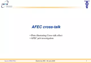
AFEC cross-talk. Plots illustrating Cross-talk effect AFEC pcb investigation. CSCs set-up. During cosmics tests in Genoa, cross-talk effect has been observed. The effect is observed like blobs of hits outside the fired region of the chamber.

E N D
AFEC cross-talk • Plots illustrating Cross-talk effect • AFEC pcb investigation Electronics WG - 09 June 2009
CSCs set-up During cosmics tests in Genoa, cross-talk effect has been observed. The effect is observed like blobs of hits outside the fired region of the chamber. The detector system is realized with a sandwich of three chambers, 2 CSCs type 1P and 1 CSC type 1G. Some plots will be illustrated concerning the 1P type chamber positioned in the middle of the sandwich. The plots are obtained from high-statistics (~117k events) cosmics run. Electronics WG - 09 June 2009
2D diagrams log(z) version of the first Wire Wire cluster Each wire cluster fitting a cosmics track in the telescope, all wire hits recorded are plotted as a function of the cluster center. There are two "blobs" out of the diagonal. Electronics WG - 09 June 2009
2D diagrams 68.5 71.5 Zoom around the largest blob. Electronics WG - 09 June 2009
1D plots ? ? A couple of 1D plots of y-projections in the region of the blob, among those with the highest level of cross-talk. Electronics WG - 09 June 2009
C12 C13 1n 1p TRIGGER[8:1] 6kV CH_1 TRIGGER LOGIC [16:1] R12 R13 10k 330 T1 0 0 DAV_A1 VFAT_1 ANODES[128:1] DOUT_A1 MEZZANINE CK40 DACo_I_A1 DACo_V_A1 I2C_VFAT (MAX 8) TRIGGER[16:9] ANODES[256:1] INPUTS DAV_A2 VFAT_2 ANODES[256:129] DOUT_A2 MEZZANINE DACo_I_A2 DACo_V_A2 2V5D 2V5A POWER_SUPPLY POWER_SUPPLY DAC_V_A2 DAC_I_A2 DAC_V_A1 C14 C15 CH_256 DAC_I_A1 1n 1p 6kV R14 R15 10k 330 0 0 Anode FECard block diagram 1nF 2.7pF Victims 10k 10k Aggressors 1nF 2.7pF Definitions: Aggressor signal after HV capacitor. Victim VFAT input. 10k 10k Electronics WG - 09 June 2009
AFEC 1P type layout 1 32 33 64 65 96 97 127 4 layers: Top VFAT fan-out and shield. INT1 Signal routing. INT2 Signal routing Bottom Shield. Electronics WG - 09 June 2009
Top plusINT1 Diagram blob 72 65 85 Electronics WG - 09 June 2009
Top plusINT1, blob layout zoom 69 aggressor 85 victim 69 72 • 72 aggressor • 85 victim • 89 victim 85 89 Exists correlation with the diagrams shown before. Electronics WG - 09 June 2009
Conclusions • Only one out of several AFEC layout points analyzed have been presented. • The correlation between the cross-talk observed from the data acquired and the layout routing is demonstrated. • The “blobs” aren’t big, they involve 3-4 channels max. • They are distributed along the AFEC pcb 10% of events could have a ghost active channel. • Phenomena observed also between internal layers INT2 and INT3 where the shield plane is absent. • Data taking in progress for the 1G-type. • Preliminary AFEC PCBs check have evidenced that each pcb type have some critical points (possible “blobs”). Electronics WG - 09 June 2009
Solution(s) • Increase the AFEC pcb stack-up from 4 to 6 layers. • This modification insert two extra ground shield planes between TopINT1, and INT1INT2. • This structure, signal planes interleaved with gnd planes have been adopted for the CFEC layout design with excellent results. • Confirmed also by the AFEC itself, in the areas where the traces are well shielded. • Starting now with the production, we will get the new PCBs ready to be mounted on the CSCs at end of July. • Material procurement in progress. • HV capacitors • Panasonic connectors available. • Off line analysis • Aggressor Victim is always unidirectional possible mask table. Electronics WG - 09 June 2009