Download
1 / 45
490 likes | 650 Views
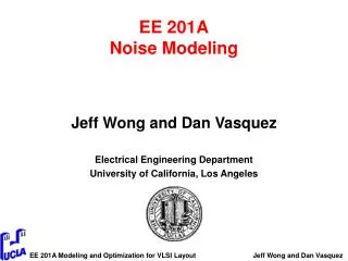
EE 201A Noise Modeling. Jeff Wong and Dan Vasquez Electrical Engineering Department University of California, Los Angeles. Efficient Coupled Noise Estimation for On-Chip Interconnects. Anirudh Devgan Austin Research Laboratory IBM Research Division, Austin TX. Motivation.

E N D
EE 201ANoise Modeling • Jeff Wong and Dan Vasquez • Electrical Engineering Department • University of California, Los Angeles
Efficient Coupled Noise Estimation for On-Chip Interconnects Anirudh Devgan Austin Research Laboratory IBM Research Division, Austin TX
Motivation • Noise failure can be more severe than timing failure • Difficult to control from chip terminals • Expensive to correct (refabrication) • Circuit or timing simulation (like SPICE) can be used • Linear reduction techniques can be applied for linearly modeled circuits • i.e. moment matching methods • Inefficient for noise verification and avoidance applications
Noise Estimation • The paper presents an electrical metric for efficiently estimating coupled noise for on-chip interconnects • Capacitive coupling between an aggressor net and a victim net leads to coupled noise • Aggressor net: switches states; source of noise for victim net • Victim net: maintains present state; affected by coupled noise from aggressor net
Circuit Schematic Coupling capacitors CC = [CC,ii] V2,1 V2,n C2 = [C2,ii] V1,1 V1,n Switching signal Vs(t) C1 = [C1,ii] • Let’s analyze the case for one aggressor net and one victim net
Circuit Equations • Coupled equation for circuit: • In Laplace domain:
Circuit Equations • Aggressor net: • Victim net:
Transfer Function • Transfer function: • Simplifications (details later): • Simplified transfer function:
Simplifications • A12 = 0 • No resistive (or DC) path exists from the aggressor net to the victim net • A21 = 0 • No resistive (or DC) path exists from the victim net to the aggressor net • B2 = 0 • No resistive (or DC) path exists from the voltage/noise source to the victim net
Maximum Induced Noise • H(s=0) = 0 • Coupling between aggressor and victim net is purely capacitive • Maximum induced noise can be computed • Assume Vs is a finite or infinite ramp
Maximum Induced Noise • Final value theorem: • Ramp input u(s):
Circuit Interpretation Switching slope
Circuit Computations(matrix method) • Step 1: Compute • Requires circuit analysis of the aggressor net • Step 2: Compute • Requires a matrix multiplication • Step 3: Compute • Requires circuit analysis of the victim net
Circuit Computations(by inspection) • Step 1: Compute • Aggressor circuit transformation: • Replace input source with it’s derivative • Replace aggressor net’s capacitors with open circuits
Circuit Computations (by inspection) • Step 1: Compute • Typical interconnects: • Negligible loss: no resistive path to ground
Circuit Computations (by inspection) • Step 2: Compute • Convert steady state derivative on the aggressor net to a current on the victim net • i: index of node on the victim net • j: index of node on the aggressor net
Circuit Computations (by inspection) • Step 3: Compute • Victim circuit transformation: • Replace capacitors with coupling currents • The voltage at each node corresponds to that node’s maximum induced noise
Circuit Computations (by inspection) • Step 3: Compute • Typical interconnects: • Compute by inspection in linear time
Circuit Computations (by inspection) • Step 3: Compute • 3RC Circuit example:
Computation Costs • Step 1: • No computation required • Step 2: • Simple multiplications • Step 3: • Simple multiplications • Multiple aggressor nets: • Coupling currents from step 2 determined from a linear superposition
Experiment • Typical small RC interconnect structure • Rise time of 200 ps or 100 ps • Power supply voltage of 1.8 V • Conventional circuit simulation vs. proposed metric • Run-time comparisons for various circuit sizes
Accuracy Results • 10 nodes, 200 ps rise time
Accuracy Results • 10 nodes, 100 ps rise time
Accuracy Results • Metric accuracy degrades with reduction in rise times • Metric estimation is more conservative than circuit model’s • Fast rise times don’t allow circuit to reach ramp steady state noise • Loading of interconnect normally does not allow for very small rise times • Metric accuracy should be acceptable for many applications
Run-time Results • Arnoldi-based model reduction used a matrix solution to compute circuit response • Requires repeated factorizations, eigenvalue calculations, and time exponential evaluations
Conclusions • The proposed metric determines an upper bound on coupled noise for RC and over-damped RLC interconnects • Metric becomes less accurate as rise time decreases • The proposed metric is much more run-time efficient than circuit modeling methods
Improved Crosstalk Modeling for Noise Constrained Interconnect Optimization Jason Cong, David Zhigang Pan & Prasanna V. Srinivas Department of Computer Science, UCLA Magma Design Automation, Inc. 2 Results Way, Cupertino, CA 95014
Motivation • Deep sub-micron net designs have higher aspect ratio (h/w) • Increased coupling capacitance between nets • Longer propagation delay • Increased logic errors --- Noise • Reduced noise margins • Lower supply voltages • Dynamic Logic • Crosstalk cannot be ignored
Aggressor / Victim Network Aggressor Victim • Assuming idle victim net • Ls: Interconnect length before coupling • Lc: Interconnect length of coupling • Le: Interconnect length after coupling • Aggressor has clock slew tr
2- Model Rise time victim / aggressor coupling capacitance • Victim net is modeled as 2 -RC circuits • Rd: Victim drive resistance • Cx is assumed to be in middle of Lc
2- Model Parameters Aggressor Victim
Analytical Solution part 2 • s-domain output voltage • Transform function H(s)
Analytical Solution part 3 • Aggressor input signal • Output voltage
Simplification of Closed Form Solution • Closed form solution complicated • Non-intuitive • Noise peak amplitude, noise width? • Dominant-pole simplification
Dominant-Pole Simplification RC delay from upstream resistance of coupling element Elmore delay of victim net
Intuition of Dominant Pole Simplification • vout rises until tr and decays after • vmax evaluated at tr
Extension to RC Trees • Similar to previous model with addition of lumped capacitances
Results • Average errors of 4% • 95% of nets have errors less than 10%
Spice Comparison peak noise noise width
Effect of Aggressor Location • As aggressor is moved close to receiver, peak noise is increased Ls varies from 0 to 1mm Lc has length of 1mm Le varies from 1mm to 0
Optimization Rules • Rule 1: • If RsC1 < ReCL • Sizing up victim driver will reduce peak noise • If RsC1 > ReCL and tr << tv • Driver sizing will not reduce peak noise • Rule 2: • Noise-sensitive victims should avoid near-receiver coupling
Optimization Rules part 2 • Rule 3: • Preferred position for shield insertion is near a noise sensitive receiver • Rule 4: • Wire spacing is an effective way to reduce noise • Rule 5: • Noise amplitude-width product has lower bound • And upper bound
Conclusions • 2- model achieves results within 6% error of HSPICE simulation • Dominant node simplification gives intuition to important parameters • Design rules established to reduce noise
References • Anirudh Devgan, “Efficient Coupled Noise Estimation for On-chip Interconnects”, ICCAD, 1997. • J. Cong, Z. Pan and P. V. Srinivas, “Improved Crosstalk Modeling for Noise Constrained Interconnect Optimization”, Proc. Asia South Pacific Design Automation Conference (ASPDAC), Jan. 30 - Feb. 2, 2001, Pacifico Yokohama, Japan.