Chapter 6 Mixers
1.84k likes | 3.34k Views
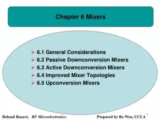
Chapter 6 Mixers. 6.1 General Considerations 6.2 Passive Downconversion Mixers 6.3 Active Downconversion Mixers 6.4 Improved Mixer Topologies 6.5 Upconversion Mixers. Behzad Razavi, RF Microelectronics. Prepared by Bo Wen, UCLA. Chapter Outline. Conversion Gain Noise Input Impedance

Chapter 6 Mixers
E N D
Presentation Transcript
Chapter 6 Mixers • 6.1 General Considerations • 6.2 Passive Downconversion Mixers • 6.3 Active Downconversion Mixers • 6.4 Improved Mixer Topologies • 6.5 Upconversion Mixers Behzad Razavi, RF Microelectronics. Prepared by Bo Wen, UCLA
Chapter Outline • Conversion Gain • Noise • Input Impedance • Current-Driven Mixers • Conversion Gain • Noise • Linearity • Mixer Noise Figures • Port-to-Port Feedthrough • Single-Balanced and Double-Balanced Mixers • Passive and Active Mixers Improved Mixer Topologies General Considerations Active Mixers Upconversion Mixers Passive Mixers • Active Mixers with Current Source Helpers • Active Mixers with High IP2 • Active Mixers with Low Flicker Noise • Conversion Gain • Noise • Linearity
General Considerations • Mixers perform frequency translation by multiplying two waveforms (and possibly their harmonics). The LO port of this mixer is very nonlinear. The RF port, of course, must remain sufficiently linear to satisfy the compression and/or intermodulation requirements.
Performance Parameters: Noise and Linearity, Gain • Noise and Linearity: The design of downconversion mixers entails a compromise between the noise figure and the IP3 (or P1dB). In a receive chain, the input noise of the mixer following the LNA is divided by the LNA gain when referred to the RX input. Similarly, the IP3 of the mixer is scaled down by the LNA gain. • Gain: mixer gain is critical in suppression of noise while retaining linearity. Downconversion mixers must provide sufficient gain to adequately suppress the noise contributed by subsequent stages. However, low supply voltages make it difficult to achieve a gain of more than roughly 10 dB while retaining linearity.
Performance Parameters: Port-to-Port Feedthrough • Owing to device capacitances, mixers suffer from unwanted coupling (feedthrough) from one port to another. In figure above, the gate-source and gate-drain capacitances create feedthrough from the LO port to the RF and IF ports. In the direct-conversion receiver: LO-RF feedthrough is entirely determined by the symmetry of the mixer circuit and LO waveforms. The LO-IF feedthrough is heavily suppressed by the baseband low-pass filter(s).
Example of LO-RF Feedthrough in Mixer Consider the mixer shown below, where VLO = V1 cos ωLOt + V0 and CGS denotes the gate-source overlap capacitance of M1. Neglecting the on-resistance of M1 and assuming abrupt switching, determine the dc offset at the output for RS = 0 and RS > 0. Assume RL >> RS. The LO leakage to node X is expressed as Exhibiting a magnitude of 2 sin(π/2)/π =2/π, this harmonic can be expressed as (2/π)cosωLOt, yielding The dc component is therefore equal to The As expected, the output dc offset vanishes if RS = 0.
Generation of DC Offset: an Intuitive Perspective Suppose, as shown below, the RF input is a sinusoid having the same frequency as the LO. • Each time the switch turns on, the same portion of the input waveform appears at the output, producing a certain average.
Effect of Feedthrough in Direct-Conversion and Heterodyne RX Direct-Conversion RX: • A large in-band interferer can couple to the LO and injection-pull it, thereby corrupting the LO spectrum. • The RF-IF feedthrough corrupts the baseband signal by the beat component resulting from even-order distortion in the RF path. Heterodyne RX: • Here, the LO-RF feedthrough is relatively unimportant • The LO-IF feedthrough, becomes serious if ωIF and ωLOare too close to allow filtering of the latter.
Port-to-Port Feedthrough in Half-RF RX Shown below is a receiver architecture wherein ωLO= ωRF/2 so that the RF channel is translated to an IF of ωRF- ωLO = ωLOand subsequently to zero. Study the effect of port-to-port feedthroughs in this architecture. For the RF mixer, the LO-RF feedthrough is unimportant as it lies at ωRF/2 and is suppressed. Also, the RF-LO feedthrough is not critical because in-band interferers are far from the LO frequency, creating little injection pulling. The RF-IF feedthrough proves benign because low-frequency beat components appearing at the RF port can be removed by high-pass filtering. The most critical feedthrough in this architecture is that from the LO port to the IF port of the RF mixer. Since ωIF= ωLO, this leakage lies in the center of the IF channel, potentially desensitizing the IF mixers (and producing dc offsets in the baseband.). The IF mixers also suffer from port-to-port feedthroughs.
Mixer Noise Figures: SSB Noise Figure For simplicity, let us consider a noiseless mixer with unity gain. • The mixer exhibits a flat frequency response at its input from the image band to the signal band. • The noise figure of a noiseless mixer is 3 dB. This quantity is called the “single-sideband” (SSB) noise.
Mixer Noise Figures: DSB Noise Figure Now, consider the direct-conversion mixer shown below. • In this case, only the noise in the signal band is translated to the baseband, thereby yielding equal input and output SNRs if the mixer is noiseless. • The noise figure is thus equal to 0 dB. This quantity is called the “double-sideband” (DSB) noise figure
Noise Behavior in Heterodyne Receiver (Ⅰ) A student designs the heterodyne receiver shown below for two cases: (1) ωLO1is far from ωRF; (2) ωLO1lies inside the band and so does the image. Study the noise behavior of the receiver in the two cases. Solution: In the first case, the selectivity of the antenna, the BPF, and the LNA suppresses the thermal noise in the image band. Of course, the RF mixer still folds its own noise. The overall behavior is illustrated below, where SA denotes the noise spectrum at the output of the LNA and Smix the noise in the input network of the mixer itself. Thus, the mixer downconverts three significant noise components to IF: the amplified noise of the antenna and the LNA around ωRF, its own noise around ωRF, and its image noise around ωim.
Noise Behavior in Heterodyne Receiver (Ⅱ) A student designs the heterodyne receiver shown below for two cases: (1) ωLO1is far from ωRF; (2) ωLO1lies inside the band and so does the image. Study the noise behavior of the receiver in the two cases. Solution: In the second case, the noise produced by the antenna, the BPF, and the LNA exhibits a flat spectrum from the image frequency to the signal frequency. As shown on the right, the RF mixer now downconverts four significant noise components to IF: the output noise of the LNA around ωRFand ωim, and the input noise of the mixer around ωRFand ωim. We therefore conclude that the noise figure of the second frequency plan is substantially higher than that of the first. In fact, if the noise contributed by the mixer is much less than that contributed by the LNA, the noise figure penalty reaches 3 dB. The low-IF receivers of Chapter 4, on the other hand, do not suffer from this drawback because they employ image rejection.
NF of Direct-Conversion Receivers It is difficult to define a noise figure for receivers that translate the signal to a zero IF. • This is the most common NF definition for direct-conversion receivers. • The SNR in the final combined output would serve as a more accurate measure of the noise performance, but it depends on the modulation scheme.
Example of Noise Spectrum of a Simple Mixer (Ⅰ) Consider the simple mixer shown below. Assuming RL >> RS and the LO has a 50% duty cycle, determine the output noise spectrum due to RS, i.e., assume RL is noiseless. Solution: Since Vout is equal to the noise of RS for half of the LO cycle and equal to zero for the other half, we expect the output power density to be simply equal to half of that of the input, i.e., 2kTRS. To prove this conjecture, we view Vn,out(t) as the product of Vn,RS(t) and a square wave toggling between 0 and 1. The output spectrum is thus obtained by convolving the spectra of the two. (shown in next slide)
Example of Noise Spectrum of a Simple Mixer (Ⅱ) The output spectrum consists of (a) 2kTRS × 0.52, (b) 2kTRS shifted to the right and to the left by ± fLO and multiplied by (1/π)2, (c) 2kTRS shifted to the right and to the left by ± 3fLO and multiplied by [1/(3π)]2, etc. We therefore write It follows that the two-sided output spectrum is equal to kTRS and hence the one-sided spectrum is given by
Single-Balanced Mixers The simple mixer previously discussed operate with a single-ended RF input and a single-ended LO. Discarding the RF signal for half of the LO period. • Figure above (left) depicts a more efficient approach whereby two switches are driven by differential LO phases, thus “commutating” the RF input to the two outputs. Called a “single-balanced” mixer. • As seen in figure above (right), the LO-RF feedthrough at ωLOvanishes if the circuit is symmetric
Double-Balanced Mixers • We connect two single-balanced mixers such that their output LO feedthroughs cancel but their output signals do not. • Called a “double-balanced” mixer, the circuit above operates with both balanced LO waveforms and balanced RF inputs.
Ideal LO Waveform • The LO waveform must ideally be a square wave to ensure abrupt switching and hence maximum conversion gain. • At very high frequencies, the LO waveforms inevitably resemble sinusoids. • Downconversion of interferers located at the LO harmonics is a serious issue in broadband receiver.
Passive Downconversion Mixers: Gain • The conversion gain in figure below is equal to 1/π for abrupt LO switching. • We call this topology a “return-to-zero” (RZ) mixer because the output falls to zero when the switch turns off. Explain why the mixer above is ill-suited to direct-conversion receivers. Since the square wave toggling between 0 and 1 carries an average of 0.5, VRF itself also appears at the output with a conversion gain of 0.5. Thus, low-frequency beat components resulting from even-order distortion in the preceding stage directly go to the output, yielding a low IP2.
Example of Downconversion Gain of Single-Balanced Topology Determine the conversion gain if the circuit of figure above is converted to a single-balanced topology. Solution: As illustrated in figure above, the second output is similar to the first but shifted by 180 °. Thus, the differential output contains twice the amplitude of each single-ended output. The conversion gain is therefore equal to 2/π (≈ -4 dB). Providing differential outputs and twice the gain, this circuit is superior to the single-ended topology above.
Example of Downconversion Gain of Double-Balanced Topology Determine the voltage conversion gain of a double-balanced version of the above topology. (Decompose the differential output to return-to-zero waveforms.) Solution: In this case, Vout1 is equal to VRF+for one half of the LO cycle and equal to VRF- for the other half, i.e, R1 and R2 can be omitted because the outputs do not “float.” We observe that Vout1 - Vout2 can be decomposed into two return-to-zero waveforms, each having a peak amplitude of 2V0. Since each of these waveforms generates an IF amplitude of (1/π)2V0 and since the outputs are 180 ° out of phase, we conclude that Vout1 - Vout2contains an IF amplitude of (1/π)(4V0). Noting that the peak differential input is equal to 2V0, we conclude that the circuit provides a voltage conversion gain of 2/π, equal to that of the single-balanced counterpart.
Sampling Mixer: the Idea • If the resistor is replaced with a capacitor, such an arrangement operates as a sample-and-hold circuit and exhibits a higher gain because the output is held—rather than reset—when the switch turns off. The output waveform of figure on the right (top) can be decomposed into two as figure at bottom.
Sampling Mixer: Conversion Gain (Ⅰ) We first recall the following Fourier transform pairs: Since y1(t) is equal to x(t) multiplied by a square wave toggling between zero and 1, and since such a square wave is equal to the convolution of a square pulse and a train of impulses shown below,
Sampling Mixer: Conversion Gain (Ⅱ) The component of interest in Y1(f) lies at the IF and is obtained by setting k to ± 1 As expected, the conversion gain from X(f) to Y1(f) is equal to 1/π, but with a phase shift of 90°.
Sampling Mixer: Conversion Gain (Ⅲ) The second output, y2(t), can be viewed as a train of impulses that sample the input and are subsequently convolved with a square pulse: Figure below depicts the spectrum, revealing that shifted replicas of X(f) are multiplied by a sinc envelope.
Sampling Mixer: Conversion Gain (Ⅳ) The component of interest in Y2(f) is obtained by setting k to ± 1 If the IF is much lower than 2fLO The total IF output is therefore equal to • If realized as a single-balanced topology, the circuit provides a gain twice this value. • Though a passive circuit, the single-ended sampling mixer actually has a voltage conversion gain greater than unity.
Example of the Voltage Conversion Gain of Double-Balanced Sampling Mixer Determine the voltage conversion gain of a double-balanced sampling mixer. Solution: The capacitors play no role here because each output is equal to one of the inputs at any given point in time. The conversion gain is therefore equal to 2/π, about 5.5 dB lower than that of the single-balanced topology discussed above.
Output Current Combining of Two Single-Band Mixers • If necessary, double-balanced operation can be realized through the use of two single-balanced mixers whose outputs are summed in the current domain. • In this case, the mixer conversion gain is still equal to 1.48 dB.
LO Self-Mixing • Due to the nonlinearity of CGS1 and CGS2 arising from large LO amplitudes, VP does change with time but only at twice the LO frequency. • Upon mixing with the LO signal, this component is translated to fLO and 3fLO—but not to dc. • In practice, however, mismatches between M1 and M2 and within the oscillator circuit give rise to a finite LO leakage to node P.
Noise The output noise is given by 4kT(Ron||RL) when S1 is on and by 4kTRL when it is off. On the average, If we select Ron << RL to minimize the conversion loss, Dividing the result by 1/π2 If Ron = 100 Ωand RL = 1 kΩ, determine the input-referred noise of the above RZ mixer. Solution: This noise would correspond to a noise figure of 10 log[1+ (8.14/0.91)2] = 19 dB in a 50-Ω system.
Noise Spectrum of Sampling Mixer: Three Observations • First, in the simple circuit on the right, if Vin = 0, • We say the noise is “shaped” by the filter. • Second, in the switching circuit on the right, the output is equal to the shaped noise of R1 when S1 is on and a sampled, constant value when it is off. • Third, we can decompose the output into two waveforms Vn1 and Vn2 as shown on the right.
Noise Spectrum of Sampling Mixer: Spectrum of Vn1 We view this waveform as the product of Vn,LPF (t) and a square wave toggling between 0 and 1. In practice, the sampling bandwidth of the mixer, 1/(R1C1), rarely exceeds 3ωLO, and hence At low output frequencies, this expression reduces to: Note that this is the two-sided spectrum.
Noise Spectrum of Sampling Mixer: Spectrum of Vn2 The sum of these aliased components is given by For the summation in equation above, we have
Noise Spectrum of Sampling Mixer: Correlation Between Vn1 and Vn2 (Ⅰ) • The correlation arises from two mechanisms: • (1) as the circuit enters the track mode, the previous sampled value takes a finite time to vanish • (2) when the circuit enters the hold mode, the frozen noise value, Vn2, is partially correlated with Vn1. • The former mechanism is typically negligible. • For the latter, we recognize that the noise frequency components far below fLO remain relatively constant during the track and hold modes.
Noise Spectrum of Sampling Mixer: Correlation Between Vn1 and Vn2 (Ⅱ) Summing the one-sided spectra of Vn1 and Vn2 and the low-frequency contribution, 4kTR1, gives the total (one-sided) output noise at the IF: The input-referred noise is obtained by dividing this result by 1/π2 + 1/4: The input-referred noise of a single-balanced passive (sampling) mixer is equal to For the double-balanced passive mixer
Noise of the Subsequent Stage The low gain of passive mixers makes the noise of the subsequent stage critical. As shown above (left), each common-source stage exhibits an input-referred noise voltage of Shown above (middle), the network consisting of RREF , MREF, and IREF defines the bias current of M1 and M2. Can the circuit be arranged as above (right) so that the bias resistors provide a path to remove the dc offset?
Example of DC Offset A student considers the arrangement shown in figure below (left), where Vin models the LO leakage to the input. The student then decides that the arrangement below (middle) is free from dc offsets, reasoning that a positive dc voltage, Vdc, at the output would lead to a dc current, Vdc/RL, through RL and hence an equal current through RS. This is impossible because it gives rise to a negative voltage at node X. Does the student deserve an A? Solution: The average voltage at node X can be negative. As shown above (right), VX is an attenuated version of Vin when S1 is on and equal to Vin when S1 is off. Thus, the average value of VX is negative while RL carries a finite average current as well. That is, the circuit above (middle) still suffers from a dc offset.
Input Impedance (Ⅰ) The current drawn by C1 is equal to: Taking the Fourier transform, we thus have We set k in previous discussion to zero so that X(f) is simply convolved with δ(f) expression for the input admittance:
Input Impedance (Ⅱ) If ω (the input frequency) is much less than ωLO, then the second term in the square brackets reduces to 1/2 and If ω ≈ 2πfLO(as in direct-conversion receivers), then the second term is equal to 1/(jπ) and Finally, if ω >> 2πfLO, the second term is much less than the first, yielding For the input impedance of a single-balanced mixer, If ω ≈ ωLO, then:
Flicker Noise and LO Swing • An important advantage of passive mixers over their active counterparts is their much lower output flicker noise. MOSFETs produce little flicker noise if they carry a small current, a condition satisfied in a passive sampling mixer if the load capacitance is relatively small. However, the low gain of passive mixers makes the 1/f noise contribution of the subsequent stage critical. • Passive MOS mixers require large (rail-to-rail) LO swings, a disadvantage with respect to active mixers.
Current Driven Passive Mixers: Input Impedance Voltage-driven and current-driven passive mixers entail a number of interesting differences. • First, the input impedance of the current-driven mixer shown here is quite different from that of the voltage-driven counterpart. In a passive mixer, we cannot calculate the input impedance of an LNA by applying a voltage or a current source to the input port because it is a time-variant circuit. In The input current is routed to the upper arm for 50% of the time and flows through ZBB. In the frequency domain:
Current Driven Passive Mixers: Spectra at Input and Output • The switches in figure above also mix the baseband waveforms with the LO, delivering the upconverted voltages to node A. Thus, V1(t) is multiplied by S(t) as it returns to the input, and its spectrum is translated to RF. The spectrum of V2(t) is also upconverted and added to this result.
Current Driven Passive Mixers: Noise and Nonlinearity Contribution, Duty Cycle • The second property of current-driven passive mixers is that their noise and nonlinearity contribution is reduced. • Passive mixers need not employ a 50% LO duty cycle. In fact, both voltage-driven and current driven mixers utilizing a 25% duty cycle provide a higher gain. Voltage-driven the RF current entering each switch generates an IF current given by As expected, d = 0.5 yields a gain of 2/π. More importantly, for d = 0.25, the gain reaches , 3 dB higher.
Active Downconversion Mixers: Function and Typical Realization • Mixers can be realized so as to achieve conversion gain in one stage. • Called active mixers, such topologies perform three functions: they convert the RF voltage to a current, “commutate” (steer) the RF current by the LO, and convert the IF current to voltage. • We call M2 and M3 the “switching pair.” • The switching pair does not need rail-to-rail LO swings.
Active Downconversion Mixers: Double-Balanced Topology • One advantage of double-balanced mixers over their single-balanced counterparts stems from their rejection of amplitude noise in the LO waveform.
Conversion Gain With abrupt LO switching, the circuit reduces to that shown in figure below (left). We have for R1 = R2 = RD The waveform exhibits a fundamental amplitude equal to 4/π, yielding an output given by
Active Mixer with LO at CM Level (Ⅰ) If M1 is at the edge of saturation, then For M2 to remain in saturation up to this point, its drain voltage which reduces to
Active Mixer with LO at CM Level (Ⅱ) The maximum allowable dc voltage across each load resistor is equal to Since each resistor carries half of ID1 we obtain the maximum voltage conversion gain as • Low supply voltages severely limit the gain of active mixers.
RF Current as a CM Component The conversion gain may also fall if the LO swing is lowered. • While M2 and M3 are near equilibrium, the RF current produced by M1 is split approximately equally between them, thus appearing as a common-mode current and yielding little conversion gain for that period of time. • Reduction of the LO swing tends to increase this time and lower the gain
