
Introduction
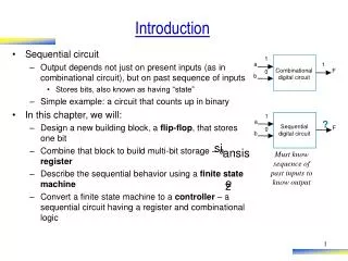
Introduction. Sequential circuit Output depends not just on present inputs (as in combinational circuit), but on past sequence of inputs Stores bits, also known as having “state” Simple example: a circuit that counts up in binary In this chapter, we will:

Introduction
E N D
Presentation Transcript
Introduction • Sequential circuit • Output depends not just on present inputs (as in combinational circuit), but on past sequence of inputs • Stores bits, also known as having “state” • Simple example: a circuit that counts up in binary • In this chapter, we will: • Design a new building block, a flip-flop, that stores one bit • Combine that block to build multi-bit storage – a register • Describe the sequential behavior using a finite state machine • Convert a finite state machine to a controller – a sequential circuit having a register and combinational logic 1 a 1 Combinational digital circuit F 0 b 1 a ? Sequential digital circuit F 0 b si ansis Must know sequence of past inputs to know output e z
SR latch S (set) Q S=0 S=1 S=0 S=0 R (reset) 0 t t t t 1 0 0 1 0 1 ecall ... 0 R X 1 0 0 Q Q Q Q R=1 R=0 R=0 R=0 1 S 0 1 R 0 1 t 0 1 Q 0 Bit Storage Using an SR Latch • Does the circuit to the right, with cross-coupled NOR gates, do what we want? • Yes! How did someone come up with that circuit? Maybe just trial and error, a bit of insight... Recall… 1 1 0 0 1 1 0 1 1 0
C all S but t on Blue lig h t C all but t on Bit Blue lig h t S t o r age C an c el Q C an c el but t on but t on R Example Using SR Latch for Bit Storage • SR latch can serve as bit storage in the example of flight-attendant call button • Call=1 : sets Q to 1 • Q stays 1 even after Call=0 • Cancel=1 : resets Q to 0 • But, there’s a problem...
Problem with SR Latch • Problem • If S=1 and R=1 simultaneously, we don’t know what value Q will take Q may oscillate. Then, because one path will be slightly longer than the other, Q will eventually settle to 1 or 0 – but we don’t know which.
A r bit r a r y SR latch circuit S X Q R Y Problem with SR Latch • Problem not just one of a user pressing two buttons at same time • Can also occur even if SR inputs come from a circuit that supposedly never sets S=1 and R=1 at same time • But does, due to different delays of different paths The longer path from X to R than to S causes SR=11 for short time – could be long enough to cause oscillation
Level-sensitive SR latch S S1 C Q R R1 S Though SR=11 briefly... Q ’ C 1 Q S R 0 1 R 0 1 C 0 1 S1 0 1 R1 0 ...S1R1 never = 11 Solution: Level-Sensitive SR Latch • Add enable input “C” as shown • Only let S and R change when C=0 • Ensure circuit in front of SR never sets SR=11, except briefly due to path delays • Change C to 1 only after sufficient time for S and R to be stable • When C becomes 1, the stable S and R value passes through the two AND gates to the SR latch’s S1 R1 inputs. Level-sensitive SR latch S X S1 Level-sensitive SR latch symbol C Clk Q R R1 Y
Level-sensitive SR latch S X S1 C Clk Q R R1 Y Clock Signals for a Latch • How do we know when it’s safe to set C=1? • Most common solution –make C pulse up/down • C=0: Safe to change X, Y • C=1: Must not change X, Y • We’ll see how to ensure that later • Clock signal -- Pulsing signal used to enable latches • Because it ticks like a clock • Sequential circuit whose storage components all use clock signals: synchronous circuit • Most common type • Asynchronous circuits – important topic, but left for advanced course
Freq Period 100 GHz 0.01 ns 10 GHz 0.1 ns 1 GHz 1 ns 100 MHz 10 ns 10 MHz 100 ns Clocks • Clock period: time interval between pulses • Above signal: period = 20 ns • Clock cycle: one such time interval • Above signal shows 3.5 clock cycles • Clock frequency: 1/period • Above signal: frequency = 1 / 20 ns = 50 MHz • 1 Hz = 1/s
D latch D S C Q R D Q ’ C Q Level-Sensitive D Latch • SR latch requires careful design to ensure SR=11 never occurs • D latch relieves designer of that burden • Inserted inverter ensures R always opposite of S D latch symbol
Clk Problem with Level-Sensitive D Latch • D latch still has problem (as does SR latch) • When C=1, through how many latches will a signal travel? • Depends on for how long C=1 • Clk_A -- signal may travel through multiple latches • Clk_B -- signal may travel through fewer latches • Hard to pick C that is just the right length • Can we design bit storage that only stores a value on the rising edge of a clock signal? rising edges
rising edges Clk D flip-flop D latch D latch Q ’ D Dm Qm Ds Q s ’ Q Cs C m Qs master servant Clk D Flip-Flop • Flip-flop: Bit storage that stores on clock edge, not level • One design -- master-servant • Two latches, output of first goes to input of second, master latch has inverted clock signal • So master loaded when C=0, then servant when C=1 • When C changes from 0 to 1, master disabled, servant loaded with value that was at D just before C changed -- i.e., value at D during rising edge of C Note: Hundreds of different flip-flop designs exist
rising edges Clk D Q ’ Q D Flip-Flop Internal design: Just invert servant clock rather than master D Q ’ The triangle means clock input, edge triggered Q Symbol for rising-edge triggered D flip-flop Symbol for falling-edge triggered D flip-flop falling edges Clk
T inside each Y D1 Q1 D2 Q2 D3 Q3 D4 Q4 w fli o l p -flop a t ches Clk Clk_A Clk_B D Flip-Flop • Solves problem of not knowing through how many latches a signal travels when C=1 • In figure below, signal travels through exactly one flip-flop, for Clk_A or Clk_B • Why? Because on rising edge of Clk, all four flip-flops are loaded simultaneously -- then all four no longer pay attention to their input, until the next rising edge. Doesn’t matter how long Clk is 1. Two latches inside each flip-flop
C all Blue light Flight attendant call-button system but t on C an c el but t on C all Blue light but t on D Q’ C an c el but t on Clk Q Flight-Attendant Call Button Using D Flip-Flop • D flip-flop will store bit • Inputs are Call, Cancel, and present value of D flip-flop, Q • Truth table shown below Preserve value: if Q=0, make D=0; if Q=1, make D=1 Circuit derived from truth table, using Chapter 2 combinational logic design process Cancel -- make D=0 Call Cancel Call -- make D=1 Q Let’s give priority to Call -- make D=1
SR latch D latch D flip-flop Level-sensitive SR latch S (set) S D S1 S D latch D latch Q ’ D Dm Qm Ds Qs’ C C Q C m Cs Qs Q Q Q master servant R Clk R R1 R (reset) Bit Storage Summary • We considered increasingly better bit storage until we arrived at the robust D flip-flop bit storage Feature: S=1 sets Q to 1, R=1 resets Q to 0. Problem: SR=11 yield undefined Q. Feature: S and R only have effect when C=1. We can design outside circuit so SR=11 never happens when C=1. Problem: avoiding SR=11 can be a burden. Feature: SR can’t be 11 if D is stable before and while C=1, and will be 11 for only a brief glitch even if D changes while C=1. Problem: C=1 too long propagates new values through too many latches: too short may not enable a store. Feature: Only loads D value present at rising clock edge, so values can’t propagate to other flip-flops during same clock cycle. Tradeoff: uses more gates internally than D latch, and requires more external gates than SR – but gate count is less of an issue today.


