
Investigation of Nanoscale Morphology and Conductivity of H-Bonded Phthalocyanine Films
This study explores the molecular assembly and electrical properties of H-bonded phthalocyanine films. By integrating amide functional groups in the side chains, we enhance intra-columnar interactions, leading to homeotropically aligned molecular structures. These structures improve charge migration in photovoltaic applications. We analyzed layered architecture through conductive probe AFM, revealing a connection between film morphology and charge injection mechanisms. Our findings indicate the potential of these films in organic photovoltaics, showcasing desirable conductivity and preliminary photovoltaic properties.

Investigation of Nanoscale Morphology and Conductivity of H-Bonded Phthalocyanine Films
E N D
Presentation Transcript
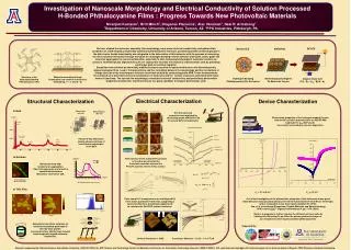
log J (mA/cm2) 10.0 nm 104 V 103 A V A 10.0 nm 102 Pc Core 15 nm Pc Core 18.1 Å 101 V2 L3 0.0 nm 100 0 nm 10-1 H H H O O O N N 10-2 N 0.0 nm C C C 10-3 10-4 voltage (mV) 10-5 S 1 μm S -1.5 -1 -0.5 0 0.5 1 1.5 S Gold 800 nm 42.3Å 4.5Å Al BCP C60 Height Histogram Pc 1.00 PEDOT-PSS 42.8Å Depth = 0.38 (±0.02) nm ITO Hist % 0.50 J (mA/cm2) 18.3Å 10 0 3.6Å 0 2 4 6 Depth (nm) 8 6 4 Absorbance Absorbance 3 µ M 2 3 3 µ µ M M 1.20 1 µ M 1 1 µ µ M M voltage (mV) 1.00 0 0.80 -0.8 -0.6 -0.4 -0.2 0 0.2 0.4 0.6 0.8 0.60 -2 A* T2eφ/kT{ e(qV/nkT) – 1} 0.40 Jtherm = -4 0.20 0.00 500 550 600 650 700 750 800 850 900 -6 JSCLC =(9/8) ε εo µ 10 nA 5 μm 0 nA Investigation of Nanoscale Morphology and Electrical Conductivity of Solution Processed H-Bonded Phthalocyanine Films : Progress Towards New Photovoltaic Materials Niranjani Kumaran1, Britt Minch2, Diogenes Placencia1, Alex Veneman1, Neal R. Armstrong1 1Department of Chemistry, University of Arizona, Tucson, AZ. 2PPG Industries, Pittsburgh, PA. We have studied the molecular assembly, film morphology, nano-scale electrical conductivity, and photovoltaic properties of a disk-shaped, peripherally substituted phthalocyanine molecule, possessing amide functional groups in the side chains. Amide functionality was integrated in the side chains of this molecule with the purpose of increasing the intra-columnar interaction through formation of a hydrogen bonding network between molecules, and to guide the columnar aggregation in a preferred direction, especially to form homeotropically aligned molecular columns on surfaces. Homeotropically aligned molecules are expected to increase the efficiency of photovoltaic cells by providing continuous path for excition migration. Deposition from solution on chemically modified surfaces resulted in layered architecture with homeotropically aligned molecular films. Local I-V characteristics and the correlation between the morphology and the mechanism of charge injection at the metal-organic interface have been studied by conducting probe AFM. These measurements have allowed us to determine electrical conductance of molecules and the contact resistance associated with metal-molecule junctions. The layered film morphology, remarkable electrical conductivity, and preliminary photovoltaic properties demonstrate that this molecule is a good candidate for organic photovoltaic cells. DEVICE MOLECULE MATERIAL Structure of the Hydrogen Bonding Phthalocyanine (Pc) Molecular assembly through Cooperative non-covalent interactions. (H-Bonding, π – π, and S - S) Hydrogen Bonding Phthalocyanine (Pc) Derivative Homeotropically Aligned Pc Molecular Layers Organic Solar Cell ITO / Pc / C60 / BCP / Al Electrical Characterization Structural Characterization Device Characterization In Bulk Monoclinic unit cell Orthorhombic unit cell Height Image Current Image Thin film electrical properties were analyzed by conducting probe AFM with Pt tip on several different substrates. Counts Photovoltaic properties of the hydrogen bonding Pc were tested with a solution processed film on PEDOT:PSS modified ITO. C60, BCP and Al top contact were added by vacuum deposition. ♦ * d = 41.8Å (100)O,M 1000 (001)O (010)O / (001)M d = 4.5 Å d = 18.0 Å 5000 Powder X-Ray Diffraction studies shows existence of two different polymorphs in the bulk * ♦ (010),M * d = 3.6 Å d = 8.8 Å ♦ 0 2θ 5 10 15 20 25 30 In Solution Hole injection at the substrate/Pc junction is found to be controlled by thermionic emission whereas the Pt-tip/Pc junction shows ohmic contact. Molecules show high tendency for aggregation. Fiber-like aggregates are formed in concentrated solutions, Monomers exist below 1µM. wavelength (nm) ln (J) ∞ V Polarized Optical Microscopy Image UV-VIS Absorption Spectroscopy In Thin Film J ∞ V2 Jsc = 2.0 mA cm-2 Voc = 0.3 mV Point contact I-V measurements on multilayered Pc films shows quantized I-V behavior, suggesting a layered architecture, providing an opportunity to calculate the Pc-HOPG contact resistance. Our initial investigation of the photovoltaic properties of this molecules shows good diode behavior and substantial photocurrent when illuminated with 100 mW/cm2 white light, and is comparable to our best, liquid crystalline Pc OPVs: Yoo, et al. International Symposium Organic Materials and Nanotechnology SPIE volume 5215 – Organic Photovoltaics IV, pp. 71-78 (2004). Work is in progress to further improve the efficiency of these cells by utilizing this H-bonding Pc as either the primary photoactive layer or as a template for other liquid crystalline phthalocyanines. Height Image Current Image Adsorption from dilute solutions on amide functionalized gold leads to layer-by-layer growth. Increased surface affinity helps to build homeotropically aligned molecular Assemblies. Supported By: Pc assembled on HOPG 1µM Pc Solution Contact Resistance = 8 MΩ Current per Molecule = ( 0.33 – 1.4 ) 104 pA Research supported by: National Science Foundation (Chemistry (CHE-0517963), the NSF Science and Technology Center for Materials and Devices for Information Technology Research (DMR-0120967), N.K. gratefully acknowledges the financial support of an Arizona Board of Regents TRIF-Photonics Graduate Fellowship.