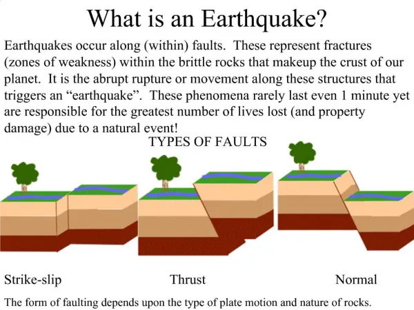
Download

1 / 99
1.02k likes | 1.28k Views
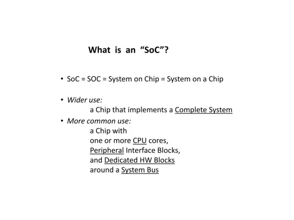
What is an “ SoC ”?. SoC = SOC = System on Chip = System on a Chip Wider use: a Chip that implements a Complete System More common use: a Chip with one or more CPU cores, Peripheral Interface Blocks, and Dedicated HW Blocks around a System Bus. What is ASIC, FPGA, SoC?.

E N D
What is an “SoC”? • SoC = SOC = System on Chip = System on a Chip • Wider use: a Chip that implements a Complete System • More common use: a Chip with one or more CPU cores,Peripheral Interface Blocks, and Dedicated HW Blocks around a System Bus
What is ASIC, FPGA, SoC? ASAAS ASAAS ASAAS ASIC FPGA SoC
Individual Gates and MemoryPre-designed All Layout except WiresPre-designed LayoutNot Pre-designed Whole ChipPre-designed Full-custom ASIC Gate-array(Structured ASIC) FPGA SoC
Inside an FPGA CLB: Configurable Logic Block
From a Designer’s Perspective • ASIC, FPGA, SoC: all the same from a designer’s point of view • We are in the SoC age => • Shop for IP blocks (IP block = Library block) • Integrate them with each other and your design
What is ASIC? • IC • Full-custom IC • IC = SP or ASSP • SP = Standard Product = Memory chip, Processor • ASSP = Application Specific Standard Product = USB interface chip for ex. • ASIC => Think of Vestel or Cisco – an equipment=box=system maker that buys ICs (SP or ASSP) puts them on a PCB. They sometimes need extra logic => hence ASIC (Application Specific Integrated Circuit)
Contemporary (wider)meaning of ASIC • Previous slide described the original (narrow) meaning of ASIC (how the word ASIC came about) • Such chips required quick methods for design because: • constraints in design time • constraints in design personnel • designs were not so aggressive • This resulted in what we call: ASIC Design Flow • Hence: an “ASIC Designer” doing “ASIC Design” may be working on an SP done in ASIC Design Flow as opposed to Full-Custom Flow.
Why/when design your own chip or customize an SoC? As opposed to taking a CPU and writing code that runs on it • BECAUSE: • CPU solution is not fast enough (FPGA is slower but offers more parallelism) • CPU is too expensive • CPU sucks too much power • CPU cannot meet the exact I/O timing requirements (no later no earlier) • CPU does not have the right number and mix of I/O pins • Form-factor: CPU is too big and/or requires a heat/sink, fan, and/or chip-set
Top Semi Companies (2011) Fabless semi Intel (USA): $50B Samsung (Korea): $29B/$260B+ TSMC (Taiwan): $15B TI (USA): $14B Toshiba (Japan): $13B/$80B Renesas (Japan): $11B Qualcomm (USA): $10B STMicro (Fr-Ita): $10B Hynix (Korea): $9B Micron (USA): $7B Broadcom (USA): $7B AMD (USA): $6B Infineon (Germany): $5B Sony (Japan): $5B/$90B Freescale (USA): $4B Elpida (Japan): $4B NXP (Holland): $4B UMC (Taiwan): $4B NVIDIA (USA): $4B Globalfoundries (USA): $4B FPGA market size $5B Fab = Foundry
Top FPGA (=PLD=CPLD) Companies(all with HQs in the USA) Xilinx: 49% Altera: 40% Lattice: 6% Microsemi (was Actel): 4% Quicklogic: 1%
ASIC Implementation Flow SW tools = $100K - $1M 3-12 months ASIC Design ~ 2 months Fabrication NRE = $100K - $4M ~ 1 month Package/Test ~ 1 month Validation
ASIC Design Flow spec(behav. code) Back-End Verification(Timing, GateSim,Formal, DRC, LVS) Front-End Design Front-End Verification Specification & Arch. Back-End Design Synthesis/Timing HDL RTL HDL RTL HDL gates Layout in GDSII
ASIC Design Tool-set Editor Back-End Verification(Timing, GateSim,Formal, DRC, LVS) Front-End Design Front-End Verification Back-End Design Synthesis/Timing HDL RTL Simulator SW Stdcell Library HDL RTL Synthesis SW HDL gates Layout in GDSII Physical design, verif., DFT/ATPG SWs
Top EDA Companies(all with HQs in the USA) • Synopsys: $1500M • Mentor Graphics: $900M • Cadence: $850M • Other: 27% • (Above are my 2010 estimates. • Total market size: $4.5B)
FPGA Design Flow spec(behav. code) Back-End Verification(Timing, GateSim,Formal, DRC, LVS) Front-End Design Front-End Verification Specification & Arch. HDL RTL HDL RTL Synthesis,Back-end,Timing Bitfile
FPGA DesignTool-set for Xilinx Front-End Design Front-End Verification HDL RTL Xilinx ISEEditor, Simulator, SynthesisAll in one IDE HDL RTL Synthesis,Back-end,Timing Bitfile
You hardly need anything you learned in your Logic coursein Modern (HDL and Synthesis based) Digital Designbecause: • We write code • We don’t design circuits • At least no gate-level circuits • We don’t care about theorems in Boolean Algebra • We don’t care about Karnaugh-maps • The synthesis SW (compiler)does the logic minimization for us • The FPGA has 1000s of gates anyway • (OK, in some extreme cases we may need to care) • Before we care about area minimizationwe need to care about meeting timing
What does RTL mean in the first place? RTL = RT-Level = Register Transfer Level
What is RT-Level digital (logic) design? Everything is a STATE MACHINE! Your (RTL) code describes the logic cloud storedVars Cloud of Logic(Combinational) more Flops storedVars_next Inputs Flop Outputs
INCREMENTER clk
0 0 0 0 INCREMENTER 0 0 1 0 clk time
0 0 0 0 INCREMENTER 0 0 1 1 clk time
0 0 0 0 INCREMENTER 1 0 0 1 clk time
0 0 0 0 INCREMENTER 1 1 0 0 clk time
0 0 0 0 INCREMENTER 1 1 1 0 clk time
0 0 0 0 INCREMENTER 1 1 1 1 clk time
0 0 1 0 INCREMENTER 0 1 0 1 clk time
Key points in this programming paradigm: • What are we programming? • How will we program? (Any guidelines?) • What is a “flop” by the way?
Flop: What is it? Edge-Triggered D-Type Flip Flop= D-Type Flip Flop= Flip-Flop = Flop Edge-Triggered Flip-Flop as opposed to: Level-Sensitive Transparent Latch = Latch
Flop: explained with WAVEFORMS posedge posedge posedge posedge clk D Q D clk Q Flop = 1-bit DigiCam
2 Flops back to back = Shift Register clk Q1 D Q2 D Q1 clk Q2
How a FLOP behaves (shown with a SHIFT REGISTER) t = before posedge clk flop1 flop2 1 0 0 1 1 1 0 1
How a FLOP behaves (shown with a SHIFT REGISTER) t = posedge clk flop1 flop2 1 1 0 0 1 1 0 1
How a FLOP behaves (shown with a SHIFT REGISTER) C2Q delay like good cholestrol t = posedge clk + C2Q delay flop1 flop2 1 1 1 0 0 1 1 0
SWITCH = LATCH Latch = Transparent Latch clk clk (= enable) D Q