Download
1 / 27
350 likes | 774 Views
EDGE EFFECTS IN REACTIVE ION ETCHING: THE WAFER- FOCUS RING GAP* Natalia Yu. Babaeva and Mark J. Kushner Iowa State University Department of Electrical and Computer Engineering Ames, IA 50011, USA natalie5@iastate.edu mjk@iastate.edu http://uigelz.ece.iastate.edu

E N D
EDGE EFFECTS IN REACTIVE ION ETCHING: THE WAFER- FOCUS RING GAP* Natalia Yu. Babaeva and Mark J. Kushner Iowa State University Department of Electrical and Computer Engineering Ames, IA 50011, USA natalie5@iastate.edu mjk@iastate.edu http://uigelz.ece.iastate.edu AVS 53rd International Symposium November 2006 * Work supported by Semiconductor Research Corp. and NSF AVS2006_Natalie_01
AGENDA • Wafer edge effects • Description of the model • Penetration of plasma into wafer-focus ring gaps in Ar/CF4 CCPs • Gap width • Focus ring conductivity • Focus ring height • Concluding remarks Iowa State University Optical and Discharge Physics AVS2006_Natalie_02
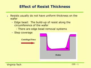
WAFER EDGE EFFECTS • Gap (< 1 mm) between wafer and focus ring in plasma tools is for mechanical clearance. • The wafer is often beveled at edge allowing for “under wafer” plasma-surface processes. • Penetration of plasma into gap can lead to deposition of contaminating films and particles. Iowa State University Optical and Discharge Physics AVS2006_Natalie_03
PENETRATION OF PLASMA INTO WAFER-FOCUS RING GAP • Penetration of plasma into wafer-focus ring gap was computationally investigated for a capacitively coupled discharge for polymerizing (Ar/CF4) conditions. • 2-dimensional model using an unstructured mesh use used to resolve multiple scale lengths. • Improvements to algorithms to revolve on momentum into gaps were made. Iowa State University Optical and Discharge Physics AVS2006_Natalie_04
nonPDPSIM CHARGED PARTICLE TRANSPORT • Poisson equation: electric potential • Transport of charged species j • Surface charge balance • Full momentum for ion fluxes • Transport of secondary electrons from biased substrate is addressed with a Monte Carlo simulation. • Neutral transport addressed with Navier-Stokes equations. Iowa State University Optical and Discharge Physics AVS2006_Natalie_05
SURFACE-KINETICS-MODULE (SKM) • SKM uses fluxes to surface to produce coverage of surface species, sticking coefficients and returning fluxes to the plasma.= • For demonstration purposes, a simple polymer depositing reaction mechanism. • Neutral deposition CFn on surfaces W producing multiple layers of polymer Polyn • Ion sputtering of polymer to generate CFn Iowa State University Optical and Discharge Physics AVS2006_Natalie_06
MESHING TO RESOLVE FOCUS RING GAP • Unstructured meshes resolve wafer-focus ring gaps of < 1 mm. Iowa State University Optical and Discharge Physics AVS2006_Natalie_07
MINMAX Pot POTENTIAL, E-FIELD, ELECTRONS • High electric field heats electrons in the sheath regions. • Off-axis maximum in [e] consequence of focus ring-uncorrelated to gap. • Ar/CF4 = 97/03, 10MHz, 90 mTorr, 300 V, 300 sccm E/n [Te] [e] Iowa State University Optical and Discharge Physics AVS2006_Natalie_08
MINMAX Log scale [Ar+] POSITIVE AND NEGATIVE IONS [CF3+] • Discharge is highly electronegative. • In spite of non-uniform [e], positive ion fluxes are fairly uniform as [M+] > [e]. • Ar/CF4 = 97/03, 10MHZ, 90 mTorr, 300 V, 300 sccm [CF3-] [F-] Iowa State University Optical and Discharge Physics AVS2006_Natalie_09
AXIAL DENSITIES • Dominant neutral polymerizing radical is CF2. • Sheaths are many mm thick which is important factor in penetration of plasma into gaps. • Ar/CF4 = 97/03, 10 MHz, 90 mTorr, 300 V, 300 sccm Iowa State University Optical and Discharge Physics AVS2006_Natalie_10
MINMAX Log scale ELECTRON PENETRATION INTO GAP 0.25 mm Gap 1.0 mm Gap • Electron penetration into gaps in anode portion of cycle is nominal due to surface charging and sheath formation. • Ar/CF4 = 97/03, 10 MHz, 90 mTorr, 300 V, 300 sccm Animation Slide Iowa State University Optical and Discharge Physics AVS2006_Natalie_11a
MINMAX Log scale ELECTRON PENETRATION INTO GAP 1.0 mm Gap 0.25 mm Gap • Electron penetration into gaps in anode portion of cycle is nominal due to surface charging and sheath formation. • Ar/CF4 = 97/03, 10 MHz, 90 mTorr, 300 V, 300 sccm Iowa State University Optical and Discharge Physics AVS2006_Natalie_11b
MINMAX Log scale Ar+ PENETRATION INTO GAP 1.0 mm Gap 0.25 mm Gap • Ions penetrate into larger gap throughout the rf cycle whose size is commensurate with sheath width. Smaller gap receives only nominal flux. • Ar/CF4 = 97/03, 10 MHz, 90 mTorr, 300 V, 300 sccm Animation Slide Iowa State University Optical and Discharge Physics AVS2006_Natalie_12a
MINMAX Log scale Ar+ PENETRATION INTO GAP 1.0 mm Gap 0.25 mm Gap • Ions penetrate into larger gap throughout the rf cycle whose size is commensurate with sheath width. Smaller gap receives only nominal flux. • Ar/CF4 = 97/03, 10 MHz, 90 mTorr, 300 V, 300 sccm Iowa State University Optical and Discharge Physics AVS2006_Natalie_12b
ION PENETRATION vs GAP SIZE • Ion penetration into gap critically depends on size relative to sheath. • Gaps ≥ sheath thickness allow penetration. • NOTE! High plasma density tools produce smaller sheaths and more penetration. • Ar/CF4 = 97/03, 10 MHz, 90 mTorr, 300 V, 300 sccm Iowa State University Optical and Discharge Physics AVS2006_Natalie_13
0.5 mm GAP: FLUXES ALONG SURFACES • Decrease of ion flux into gap is greater than decrease of neutral radical fluxes. • Negative charging of dielectric focus ring and redirection of ions helps deplete fluxes. Radicals Ions Iowa State University Optical and Discharge Physics Ar/CF4=97/03, 90 mTorr AVS2006_Natalie_14
0.5 mm GAP: POLYMER DEPOSITION • Lack of ion sputtering of polymer in gap results in disproportionately large deposition. • 100 decrease in radical flux produces only factor of 5 decrease in polymer. • Particle formation is likely to be greater. Iowa State University Optical and Discharge Physics Ar/CF4=97/03, 90 mTorr AVS2006_Natalie_15
POLYMER DEPOSITION vs GAP SIZE • When increasing gap size… Under bevel: • More radical flux penetrates while ion flux is still small. • More deposition On pedestal: • View angle to plasma enables more ion flux. • Effects are not terribly large over this range of gaps. Iowa State University Optical and Discharge Physics Ar/CF4=97/03, 90 mTorr AVS2006_Natalie_16
ION FOCUSING 0.25 mm Gap 1.0 mm Gap • Ions flux focuses on edges of wafer and focus ring: electric field enhancement and preferential negative charging. • Focusing into bevel of wafer increases with gap size. • Ar/CF4 = 97/03, 10 MHz, 90 mTorr, 300 V, 300 sccm Animation Slide Iowa State University Optical and Discharge Physics AVS2006_Natalie_17a
ION FOCUSING 0.25 mm Gap 1.0 mm Gap • Ions flux focuses on edges of wafer and focus ring: electric field enhancement and preferential negative charging. • Focusing into bevel of wafer increases with gap size. • Ar/CF4 = 97/03, 10 MHz, 90 mTorr, 300 V, 300 sccm Iowa State University Optical and Discharge Physics AVS2006_Natalie_17b
TOOL DESIGN: ION FOCUSING • Ion focusing is potentially harmful due to sputtering (etch block materials put into plasma) and erosion of pieces which reduces lifetime. • Tool design can greatly influence ion erosion. • Example: Extension of biased substrate under dielectric focus ring of differing conductivity. Iowa State University Optical and Discharge Physics AVS2006_Natalie_18
ION FOCUSING vs RING CONDUCTIVITY 0.1 Ohm-1 cm-1 10-7 Ohm-1 cm-1 • Low conductivity ring charges more negatively during anodic part of cycle; and so more focuses ion fluxes. • High conductivity ring has less focusing but allows more ion flux into gap; lack of charging reduces radial E-field. • Ar/CF4 = 97/03, 10 MHz, 90 mTorr Iowa State University Optical and Discharge Physics Animation Slide AVS2006_Natalie_19a
ION FOCUSING vs RING CONDUCTIVITY 0.1 Ohm-1 cm-1 10-7 Ohm-1 cm-1 • Low conductivity ring charges more negatively during anodic part of cycle; and so more focuses ion fluxes. • High conductivity ring has less focusing but allows more ion flux into gap; lack of charging reduces radial E-field. • Ar/CF4 = 97/03, 10 MHz, 90 mTorr Iowa State University Optical and Discharge Physics Animation Slide AVS2006_Natalie_19b
MINMAX Log scale PLASMA PENETRATION: HIGH FOCUS RING • Shielding of plasma from gap by using tall ring intensifies focusing of ions into end of ring. • Ar/CF4 = 97/03, 10 MHz, 90 mTorr, 300 V, 300 sccm Animation slide Iowa State University Optical and Discharge Physics AVS2006_Natalie_20a
MINMAX Log scale PLASMA PENETRATION: HIGH FOCUS RING • Shielding of plasma from gap by using tall ring intensifies focusing of ions into end of ring. • Ar/CF4 = 97/03, 10 MHz, 90 mTorr, 300 V, 300 sccm Iowa State University Optical and Discharge Physics AVS2006_Natalie_20b
MINMAX Log scale PLASMA PENETRATION: LOW FOCUS RING • Exposing underside of bevel by lowering focus ring allows deep ion penetration. • Ar/CF4 = 97/03, 10 MHz, 90 mTorr Iowa State University Optical and Discharge Physics AVS2006_Natalie_21
CONCLUDING REMARKS • Penetration of plasma into wafer-focus ring gap of an RIE discharge was computationally investigated. • Plasma penetration depends on size of gap relative to sheath thickness. • For test conditions (Ar/CF4, 90 mTorr, 300 V, [M+] = 1010 cm-3) significant penetration occurs for gap < 0.5 mm. • More penetration expected for high plasma densities. • Polymerization inside gap is magnified by reduction in ion sputtering. • Ion focusing into edges depends on gap size and tool design (e.g., conductivity of ring). Iowa State University Optical and Discharge Physics AVS2006_Natalie_21