Download
1 / 8
80 likes | 200 Views
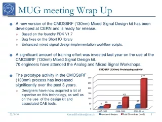
The Microelectronics User Group Meeting (MUG) held on September 30, 2011, in Vienna, Austria, focused on advancements in 130nm and 65nm technologies. Key presentations included Wojciech Bialas discussing news on 130nm technology, Vladimir Zivkovic on design flows and library aspects for the FE-I4 implementation, and Massimo Manghisoni covering noise and radiation hardness in 65nm CMOS transistors. Future plans for technology integration and access through CERN were highlighted, emphasizing user demand for improved design kits and radiation tolerance.

E N D
Microelectronics User Group MeetingWrap-up TWEPP 2011, Vienna, Austria 30/9/2011
Agenda 130 nm • “News on the 130nm Technology”by Wojciech Bialas (CERN) (10’) • “Design Toos, Flows and Library Aspects during the FE-I4 Implementation on Silicon”by Vladimir Zivkovic (NIKHEF Institute)(15’) • “Noise and Radiation Hardness of 65nm CMOS Transistors and Pixel Front-Ends”by Massimo Manghisoni (University of Bergamo)(20’) • Access of 65nm technology through CERN. by Kostas Kloukinas (CERN) (10’) 65 nm Kostas.Kloukinas@cern.ch
130nm Technology support news • Release of Mixed Signal Kit V1.8 (11/6/2011) • Based on foundry PDK V1.8.0.1 • Compatible with the “Europractice” 2011 distribution of CAE tools • Methodology for applying PDK patches. • Future Plans – driven by user demand • Expand the existing standard cell library: • Regular-Vt core cells at lower supply voltages (1.0 V, 0.8 V) • High-Vt core cells, for low power designs. • “Compact layout” core cells for area limited designs. • Rad-Tolerant cells: ex. DICE Kostas.Kloukinas@cern.ch
130 nm FEI4-A Architecture and Design Foundations • Innovations • - Region architecture (memory on pixel) • - Modular approach and distributed design • Low current operation, fault tolerance, digital and mixed-signal Test Benches for Simulation 3-2-3 Stack v v 8M 130 nm CMOS • Radiation hardness out of the box • Good power distribution • Essential when making the long columns • Substrate isolation (T3) • Essential when using standard cell synthesized logic Multi-site collaboration -> design repository necessary (SOS Cliosoft platform) Vladimir Zivkovic
65 nm Noise and radiation hardness of 65 nm CMOS transistors and pixel front-ends by Massimo Manghisoni Kostas.Kloukinas@cern.ch
65nm Technology News • CERN is actively evaluating the use of 65nm technologies for HEP applications. • The TSMC 65nm technology is a candidate technology. • Radiation Tolerance Test Results (presented at TWEPP 2011)confirms the compatibility of this technology for SLHC applications. • Negotiations are in progress with IMEC and the foundry to obtain access to IP libraries, including physical layout views, for distribution to collaborating institutes. Kostas.Kloukinas@cern.ch
65nm Technology News • The plan is to offer: • A Mixed Signal Design Kit that integrates the PDK and the IP libraries and is compatible with the workflows of the 130nm Design Kit • Provide access to memory compiler services. • Provide access to foundry services via IMEC. • MPWs, Engineering runs, Production runs. • Decide on a unique set of technology options. • Preliminary selection of Technology options: • TSMC 65nm LP (Low Power), LO (logic), with 6 metal layers. • Core vdd: 1.2V, IO vdd: 2.5V, 3.3V • NRE cost is strongly modulated by extra technology options. • Very costly to support multiple design kits. • Designers that consider the use of 65nm technology in their future projects are welcomed to contact us. Kostas.Kloukinas@cern.ch
Create a MUG mailing list • To help our communication in organizing future MUG meetings we propose to create a Microelectronics User Group mailing list. • To subscribe sent an e-mail to kostas.kloukinas@cern.ch Kostas.kloukinas@cern.ch MUG Step 3 Step 1 Step 2 Kostas.Kloukinas@cern.ch