Download
1 / 9
90 likes | 217 Views
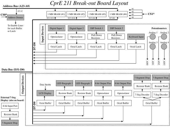
CprE 211 Break-out Board Layout. Address Demux. Digital Input 1. Octal Latch. DIP Switch 2. Octal Latch. Octal Buffer. DIP Switch 1. Octal Buffer. Octal Latch. Octal Latch. Octal Buffer. Octal Buffer. 1 MB SRAM (#3). 1 MB SRAM (#2). 1 MB SRAM (#4). Resistor Bank. Octal Buffer.

E N D
CprE 211 Break-out Board Layout Address Demux Digital Input 1 Octal Latch DIP Switch 2 Octal Latch Octal Buffer DIP Switch 1 Octal Buffer Octal Latch Octal Latch Octal Buffer Octal Buffer 1 MB SRAM (#3) 1 MB SRAM (#2) 1 MB SRAM (#4) Resistor Bank Octal Buffer Octal Buffer 1 MB SRAM (#1) Optoisolator Octal Latch Optoisolator Optoisolator Resistor Bank Resistor Bank Resistor Bank Resistor Bank Optoisolator Digital Input 2 Keyboard Input 8-bit Output Pins 8-bit Output Pins LED Bargraph 1 LED Bargraph 2 8-bit Input Port Pull-Down Resistors Pull-Down Resistors 7-Seg Decoder 7-Seg Decoder LCD Display 7-Segment Disp. 7-Segment Disp. 7-Segment Disp. Address Bus (A23-A0) #1 A5-A2 #2 CS1* CS0* #3 #4 D31-D24 D23-D16 D15-D8 D7-D0 To Enable Lines for each Buffer or Latch Potentiometers Analog 1 Analog 2 Input Devices Analog 3 Analog 4 D7-D0 AN2 AN0 AN1 AN3 Data Bus (D31-D0) Output Devices Data Strobe External 7-SegDisplay (also on board) D7-D0
5 V 5 V Address Selection for External Devices !CS2 A05 A04 Strobe Vcc Pin 1 Pin 24 A03 A Inhibit A02 B C S7 D S6 S10 Device 10 Enable S5 S11 Device 11 Enable 74HC4514 S4 S8 Device 8 Enable S3 S9 Device 9 Enable S1 S14 Device 14 Enable S2 S15 Device 15 Enable S0 S12 Device 12 Enable Gnd S13 Device 13 Enable Device 0 Enable Device 2 Enable Address Bus Device 1 Enable Device 3 Enable Device 4 Enable Device 5 Enable Device 6 Enable Device 7 Enable
5 V 5 V 5 V 5 V 7 – Segment Decoder and Display Pin 8 D05 A1 Vcc Output 5 Pin 1 Pin 16 D06 Pin 9 A2 f P0 P15 Output 6 Pin 1 Pin 16 Pin 10 !LE g P1 P14 Pin 7 !RBO a P2 P13 DM9368N Pin 6 !RBI b P3 270 W Resistor Network (8) P12 D07 Pin 4 A3 c P4 P11 Output 7 D04 Pin 2 A0 d P5 P10 Output 4 Pin 1 Gnd e P6 P9 NC P7 P8 NC Pin 8 D02 A1 P15 Output 2 Pin 1 Pin 16 D03 Pin 9 A2 f P0 P15 Output 3 Pin 1 Pin 16 Pin 10 !LE g P1 P14 Pin 7 !RBO a P2 P13 DM9368N Pin 6 !RBI b P3 270 W Resistor Network (8) P12 D01 Pin 4 A3 c P4 P11 Output 1 D00 Pin 2 A0 d P5 P10 Output 0 Pin 1 Gnd e P6 P9 NC P7 P8 NC
5 V Octal Buffer for Output Devices Device x Enable Line from Address Selection !OE1 Vcc D0 Pin 1 Pin 20 A1 !OE2 D1 A2 Y1 Output 0 D2 A3 Y2 Output 1 D3 A4 Y3 Output 2 D4 SN74AHCT541 A5 Y4 Output 3 D5 A6 Y5 Output 4 D6 A7 Y6 Output 5 D7 A8 Y7 Output 6 Gnd Y8 Output 7 Data Bus
5 V Octal Latch for Input Devices !OE Vcc Pin 1 Pin 20 D0 D0 O0 Input 0 D1 D1 O1 Input 1 D2 D2 O2 Input 2 D3 D3 O3 Input 3 SN74AHCT541 D4 D4 O4 Input 4 D5 D5 O5 Input 5 D6 D6 O6 Input 6 D7 D7 O7 Input 7 Gnd LE Device x Enable Line from Address Selection Data Bus
Pin 1 LED Bargraph Output (2 total) 5 V P0 P15 Output 0 Pin 1 Pin 16 P1 P14 Output 1 P2 P13 Output 2 P3 270 W Resistor Network (8) P12 Output 3 P4 P11 Output 4 P5 P10 Output 5 P6 P9 Output 6 P7 P8 Output 7
DIP Switch Input (2 total) 5 V Gnd P0 P15 Pin 1 Pin 16 P1 P14 P2 P13 P3 10 KW Resistor Network (8) P12 P4 P11 P5 P10 P6 P9 P7 P8 Input 0 Input 1 Input 2 Input 3 Input 4 Input 5 Input 6 Input 7
I/O Pin Header #2 5 V I/O Pin Header #4 I/O Pin Header #3 AddressSelection P0 P19 Pin 1 Pin 20 P0 P15 P1 P18 Pin 1 Pin 16 P1 P14 P2 P17 P2 P13 P3 P16 P3 P12 P4 P15 16 Pin 20 Pin P4 P11 P5 P14 P5 P10 P6 P13 P6 P9 P7 P12 P7 P8 P8 P11 P9 P10 Data Bus (D32-D0) PB-0555 Board To Enable Lines for each Buffer Or Latch I/O Pin Header #1 I/O Pin Header #2 PPC555 P0 P23 I/O Pin Header #4 Pin 1 Pin 24 P1 P22 P2 P21 Address Bus (A23-A0) P3 P20 I/O Pin Header #3 P4 P19 P5 P18 24 Pin P6 P17 I/O Pin Header #1 P7 P16 P8 P15 P9 P14 P10 P13 P11 P12