Overcoming Challenges in FPGA Initialization for DAQ Systems: A Path to Successful Data Readout
In this comprehensive overview, we detail our ambitious goals for the DAQ and MAPMT hybrid projects, the obstacles we encountered during the FPGA initialization process, and the innovative solutions we applied. Each step of the initialization sequence is outlined, from programming the FPGA and DACS to preparing the DAQ for data readout. Our testing phases with both single and dual hybrids are documented, revealing the importance of precise timing and adherence to protocols. This experience highlights our commitment to transforming challenges into successful technological advancements.

Overcoming Challenges in FPGA Initialization for DAQ Systems: A Path to Successful Data Readout
E N D
Presentation Transcript
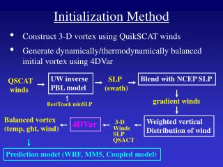
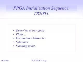
DAQ: Challenge, Dreams & Reality FPGA Initialization Sequence, TB2005. • Overview of our goals • Plans… • Encountered Obstacles • Solutions • Standing point…
PC PMC PTA Goals1 DAQ
PMC MAPMT Hybrid Goals2 Vfp Vfs Vrc Vth Dacs Chip
Plan • Initialize the FPGA on the MAPMT Hybrid • Initialize the Dacs • Initialize the ASICS • Prepare the DAQ for data readout • Test the readout chain with one hybrid • Change the DAQ to accommodate two hybrids • Test with two hybrids and more…
1. Initializing the FPGA • Load the hybrid FPGA file into the FPGA • Use slave serial mode where we shift data Serially and along with an external configuration clock (CCLK). (we are skipping here may details of the activation of this process) • If the FPGA is programmed successfully, it responds with the a specific signal that gets passed back to the PMC.
Are we really writing the right Data words into the FPGA? • We used the rising edge of the PROG Signal to start programming • the FPGA • We don’t read exactly • what we write (through Din)? • We have 17 CCLK cycles • but we are generate 16 instead OCCASIONALLY, we have a 17th clock cycle?
Check it out, write FFFF? 17 clock cycles? DIN CCLK
Understanding the Problems (PMC firmware side) Solutions • Since in the 1st PCI_CLK we latch the offset and in the 2nd we latch the data, we should make sure that we pass the data words to the FPGA bit by bit through the shift register in the 2nd Clock Cycle, not before. • As a result, we could pass just the data to the FPGA but still we had to initialize the 15th bit (which gets passed first) to zero. • Make sure we don’t shift the data words unless we are in the right conditions of the writing command (CCLK is undergoing a low to high transition). • We came up with a scenario to understand the reason behind the 17th clock cycle, we made an extensive time analysis of the CCLK generation mechanism in the PMC firmware We came up with a solution (there was a time delay issue which happens just from time to time in just some of the signals generating the clock).
Check the firmware changes with the New Labview based DAQ, It works! After Changes, We wrote 0xF0F0=1111000011110000 CCLK DIN We wrote 0x5555 = 0101010101010101 CCLK DIN
DONE • Checked the PROG signal • Checked the configuration clock: CCLK • Checked the serial data bits in”Din” • The FPGA is successfully programmed (received the expected signal from the FPGA)