
Understanding Programmable Processors: Basics & Operations
E N D
Presentation Transcript
EEE2243Digital System DesignChapter 10: Advanced Topic:Programmable Processorby Muhazam Mustapha extracted from Frank Vahid’s slides,May 2012
Learning Outcome • By the end of this chapter, students are expected to have some surface idea about the construction of programmable processor
Chapter Content • Processor • Control Unit • Instruction
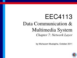
Introduction Seatbelt warning light program 3-tap FIR filter program O ther p r o g r ams Seatbelt warning light single-purpose processor • Programmable (general-purpose) processor • Mass-produced, then programmed to implement different processing tasks • Well-known common programmable processors: Pentium, Sparc, PowerPC • Lesser-known but still common: ARM, MIPS, 8051, PIC • Low-cost embedded processors found in cell phones, blinking shoes, etc. • Instructive to design a very simple programmable processor • Real processors can be much more complex e 3 2 1 I nstru c tion 0 memo r y I 2x 4 D a ta memo r y D x(t) x( t -1) x( t -2) c0 c1 c2 n-bit x t0 x t1 x t2 PC I R 2x 1 0 * * * R e g is t er file RF C o n t r oller + + r eg A L U Datapath Control unit 3-tap FIR filter single-purpose processor General-purpose processor
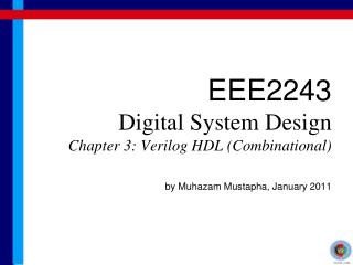
Basic Architecture • Processing generally consists of: • Loading some data • Transforming that data • Storing that data • Basic datapath: Useful circuit in a programmable processor • Can read/write data memory, where main data exists • Has register file to hold data locally • Has ALU to transform local data someh o w c onne c t ed t o the D a ta memo r y D outside w o r ld n-bit 2x 1 R e g is t er file RF A L U Datapath
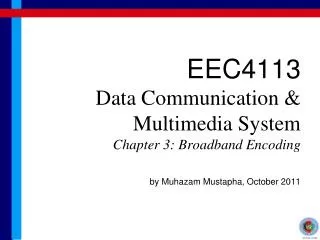
Basic Datapath Operations Load operation ALU operation Store operation • Load operation: Load data from data memory to RF • ALU operation: Transforms data by passing one or two RF register values through ALU, performing operation (ADD, SUB, AND, OR, etc.), and writing back into RF. • Store operation: Stores RF register value back into data memory • Each operation can be done in one clock cycle Data memory D Data memory D Data memory D n-bit n-bit n-bit 2x 1 2x 1 2x 1 Register file RF Register file RF Register file RF ALU ALU ALU
Basic Datapath Operations Data memory D Data memory D Data memory D n-bit n-bit n-bit 2x 1 2x 1 2x 1 Register file RF Register file RF Register file RF ALU ALU ALU Load operation ALU operation Store operation • Q: Which are valid single-cycle operations for given datapath? • Move D[1] to RF[1] (i.e., RF[1] = D[1]) • A: YES – That's a load operation • Store RF[1] to D[9] and store RF[2] to D[10] • A: NO – Requires two separate store operations • Add D[0] plus D[1], store result in D[9] • A: NO – ALU operation (ADD) only works with RF. Requires two load operations (e.g., RF[0]=D[0]; RF[1]=D[1], an ALU operation (e.g., RF[2]=RF[0]+RF[1]), and a store operation (e.g., D[9]=RF[2])
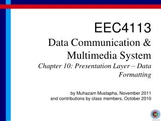
Basic Architecture 0: RF[0]=D[0] 1: RF[1]=D[1] 2: RF[2]=RF[0]+RF[1] 3: D[9]=RF[2] • D[9] = D[0] + D[1] – requires a sequence of four datapath operations: • 0: RF[0] = D[0] • 1: RF[1] = D[1] • 2: RF[2] = RF[0] + RF[1] • 3: D[9] = RF[2] • Each operation is an instruction • Sequence of instructions – program • Looks cumbersome, but that's the world of programmable processors – Decomposing desired computations into processor-supported operations • Store program in Instruction memory • Control unit reads each instruction and executes it on the datapath • PC: Program counter – address of current instruction • IR: Instruction register – current instruction Instruction memory I Data memory D n-bit x 2 1 PC IR Register file RF Controller ALU Datapath Control unit
Basic Architecture Instruction memory I 0: RF[0]=D[0] Instruction memory 1: RF[1]=D[1] I 2: RF[2]=RF[0]+RF[1] 0: RF[0]=D[0] 3: D[9]=RF[2] 1: RF[1]=D[1] Instruction memory I 2: RF[2]=RF[0]+RF[1] Data memory D 0: RF[0]=D[0] 3: D[9]=RF[2] D[0]: 99 1: RF[1]=D[1] 2: RF[2]=RF[0]+RF[1] PC R I 3: D[9]=RF[2] -> 0 1 PC R I n-bit RF[0]=D[0] 1 x 2 1 PC R I RF[0]=D[0] 1 Controller Register file RF Controller Control unit Controller a ( ) Fetch Control unit ALU b ( ) Decode Datapath Control unit Execute c ( ) • To carry out each instruction, the control unit must: • Fetch – Read instruction from inst. mem. • Decode – Determine the operation and operands of the instruction • Execute – Carry out the instruction's operation using the datapath RF[0]=D[0] R[0]: ?? 99 "load"
Basic Architecture Instruction memory I 0: RF[0]=D[0] Instruction memory 1: RF[1]=D[1] I 2: RF[2]=RF[0]+RF[1] 0: RF[0]=D[0] 3: D[9]=RF[2] 1: RF[1]=D[1] Instruction memory I 2: RF[2]=RF[0]+RF[1] Data memory D 0: RF[0]=D[0] 3: D[9]=RF[2] D[1]: 102 1: RF[1]=D[1] 2: RF[2]=RF[0]+RF[1] PC R I 3: D[9]=RF[2] -> 1 2 PC R I n-bit RF[1]=D[1] 2 x 2 1 PC R I RF[1]=D[1] 2 Controller Register file RF Controller Control unit Controller a ( ) Fetch Control unit ALU b ( ) Decode Datapath Control unit Execute c ( ) • To carry out each instruction, the control unit must: • Fetch – Read instruction from inst. mem. • Decode – Determine the operation and operands of the instruction • Execute – Carry out the instruction's operation using the datapath RF[1]=D[1} R[1]: ?? 102 "load"
Basic Architecture Instruction memory I 0: RF[0]=D[0] Instruction memory 1: RF[1]=D[1] I 2: RF[2]=RF[0]+RF[1] 0: RF[0]=D[0] 3: D[9]=RF[2] 1: RF[1]=D[1] Instruction memory I 2: RF[2]=RF[0]+RF[1] Data memory D 0: RF[0]=D[0] 3: D[9]=RF[2] 1: RF[1]=D[1] 2: RF[2]=RF[0]+RF[1] PC R I 3: D[9]=RF[2] -> 2 3 PC R I n-bit RF[2]=RF[0]+RF[1] 3 x 2 1 PC R I RF[2]=RF[0]+RF[1] 3 Controller Register file RF Controller 102 99 Control unit Controller 201 a ( ) Fetch Control unit ALU b ( ) Decode Datapath Control unit Execute c ( ) • To carry out each instruction, the control unit must: • Fetch – Read instruction from inst. mem. • Decode – Determine the operation and operands of the instruction • Execute – Carry out the instruction's operation using the datapath RF[2]=RF[0]+RF[1] R[2]: ?? 201 "ALU (add)"
Basic Architecture Instruction memory I 0: RF[0]=D[0] Instruction memory 1: RF[1]=D[1] I 2: RF[2]=RF[0]+RF[1] 0: RF[0]=D[0] 3: D[9]=RF[2] 1: RF[1]=D[1] Instruction memory I 2: RF[2]=RF[0]+RF[1] Data memory D 0: RF[0]=D[0] 3: D[9]=RF[2] 1: RF[1]=D[1] 2: RF[2]=RF[0]+RF[1] PC R I 3: D[9]=RF[2] -> 3 4 PC R I n-bit D[9]=RF[2] 4 x 2 1 PC R I D[9]=RF[2] 4 Controller Register file RF Controller Control unit Controller a ( ) Fetch Control unit ALU b ( ) Decode Datapath Control unit c ( ) • To carry out each instruction, the control unit must: • Fetch – Read instruction from inst. mem. • Decode – Determine the operation and operands of the instruction • Execute – Carry out the instruction's operation using the datapath D[9]=?? 201 D[9]=RF[2] R[2]: 201 "store" Execute
Basic Architecture Instruction memory I 0: RF[0]=D[0] Data memory D 1: RF[1]=D[1] 2: RF[2]=RF[0]+RF[1] 3: D[9]=RF[2] n-bit x 2 1 PC IR Register file RF Controller ALU Datapath Control unit
Sequence of Instructions • Q: Create sequence of instructions to compute D[3] = D[0]+D[1]+D[2] on earlier-introduced processor • A1: One possible sequence • First load data memory locations into register file • R[3] = D[0] • R[4] = D[1] • R[2] = D[2] • (Note arbitrary register locations) • A2: Alternative sequence • First load D[0] and D[1] and add them • R[1] = D[0] • R[2] = D[1] • R[1] = R[1] + R[2] • Next, load D[2] and add • R[2] = D[2] • R[1] = R[1] + R[2] • Next, perform the additions • R[1] = R[3] + R[4] • R[1] = R[1] + R[2] • Finally, store result • D[3] = R[1] • Finally, store result • D[3] = R[1]
Number of Cycles • Q: How many cycles are needed to execute six instructions using the earlier-described processor? • A: Each instruction requires 3 cycles – 1 to fetch, 1 to decode, and 1 to execute • Thus, 6 instr * 3 cycles/instr = 18 cycles
Three-Instruction Processor Desired program 0: RF[0]=D[0] 1: RF[1]=D[1] 2: RF[2]=RF[0]+RF[1] 3: D[9]=RF[2} Instruction memory I 0: 0000 0000 00000000 1: 0000 0001 00000001 2: 0010 0010 0000 0001 3: 0001 0010 00001001 • Instruction Set – List of allowable instructions and their representation in memory, e.g., • Load instruction—0000 r3r2r1r0 d7d6d5d4d3d2d1d0 • Store instruction—0001 r3r2r1r0 d7d6d5d4d3d2d1d0 • Add instruction—0010 ra3ra2ra1ra0 rb3rb2rb1rb0 rc3rc2rc1rc0 Instructions in 0s and 1s – machine code opcode operands
Three-Instruction Program Desired program 0: RF[0]=D[0] 1: RF[1]=D[1] 2: RF[2]=RF[0]+RF[1] 3: D[9]=RF[2} Computes D[9] = D[0] + D[1] Instruction memory I 0: 0000 0000 00000000 Data memory D 1: 0000 0001 00000001 2: 0010 0010 0000 0001 3: 0001 0010 00001001 n-bit × 2 1 PC R I Register file RF Controller ALU Datapath Control unit
Three-Instruction Program • Another example program in machine code • Compute D[5] = D[5] + D[6] + D[7] • Load instruction—0000 r3r2r1r0 d7d6d5d4d3d2d1d0 • Store instruction—0001 r3r2r1r0 d7d6d5d4d3d2d1d0 • Add instruction—0010 ra3ra2ra1ra0 rb3rb2rb1rb0 rc3rc2rc1rc0
Assembly Code Desired program 0: RF[0]=D[0] 1: RF[1]=D[1] 0: 0000 0000 00000000 2: RF[2]=RF[0]+RF[1] 1: 0000 0001 00000001 3: D[9]=RF[2] 2: 0010 0010 0000 0001 3: 0001 0010 00001001 • Machine code (0s and 1s) hard to work with • Assembly code – Uses mnemonics • Load instruction—MOV Ra, d • specifies the operation RF[a]=D[d]. a must be 0,1, ..., or 15—so R0 means RF[0], R1 means RF[1], etc. d must be 0, 1, ..., 255 • •Store instruction—MOV d, Ra • specifies the operation D[d]=RF[a] • •Add instruction—ADD Ra, Rb, Rc • specifies the operation RF[a]=RF[b]+RF[c] 0: MOV R0, 0 1: MOV R1, 1 2: ADD R2, R0, R1 3: MOV 9, R2 machine code assembly code
Six-Instruction Processor • Let's add three more instructions: • Load-constant instruction—0011 r3r2r1r0 c7c6c5c4c3c2c1c0 • MOV Ra, #c—specifies the operation RF[a]=c • Subtract instruction—0100 ra3ra2ra1ra0 rb3rb2rb1rb0 rc3rc2rc1rc0 • SUB Ra, Rb, Rc—specifies the operation RF[a]=RF[b] –RF[c] • Jump-if-zero instruction—0101 ra3ra2ra1ra0 o7o6o5o4o3o2o1o0 • JMPZ Ra, offset—specifies the operation PC = PC + offset if RF[a] is 0
Six-Instruction Program • Example program – Count number of non-zero words in D[4] and D[5] • Result will be either 0, 1, or 2 • Put result in D[9]