Download
1 / 17
170 likes | 290 Views
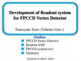
Development of Readout ASIC for FPCCD Vertex Detector. 01 October 2009 Kennosuke.Itagaki Tohoku University. FPCCD Vertex Detector. 120mm. e +. e +. e -. e -. Large amounts of e + ・ e - pair background is generated at beam collision.

E N D
Development of Readout ASIC for FPCCD Vertex Detector 01 October 2009 Kennosuke.Itagaki Tohoku University
FPCCD Vertex Detector 120mm e+ e+ e- e- • Large amounts of e+・e-pair background is generated at beam collision. • For low pixel occupancy, we develop Vertex Detector adopt fine pixel CCD sensor. • FPCCDVertex Detector • Fine Pixel CCD • Pixel size : 5mm × 5mm • Epitaxial layer thickness:15mm • 20,000 ×128 pix/ch • # of channels~ 6,000ch • Double layers : CCDs are attached on two sides of the ladders. • Readout ASIC for FPCCD is developed. g e+ g e-
Requirements to readout ASIC ~1ms ~200ms • Power consumption< 6 mW/ch • Setting in a cryostat • Total power consumption < 100W • Readout rate> 10 Mpix/sec • Read out in the inter-train time • 20,000 ×128 pix / 200 ms • Noise level < 30 electrons • Signal becomes small for particles penetrating with large angle. • Readout ASIC was designed to satisfy these requirement. pixel Signal is small
Solution of Requirements • Power consumption< 6 mW/ch • ADC is the main power consumption source. • For suppressing power consumption at ADC, charge sharing ADC is used. • Signal is converted by comparing • the reference voltage with a capacitor. • Power consumption of ADC < 10μW/ch • Readout rate> 10 Mpix/sec • It is difficult to operate charge sharing ADC with high-speed • Two 5MHzADC are used alternatively. • 10Mpix/sec • Estimated noise level < 30e
Test sample of readout ASIC sampling • Design of prototype ASIC • Amplifier • Low pass filter (LPF) • Correlated double sampling (CDS) • sample backward and forward of pixel data • output voltage difference at sampling points • Charge sharing ADC×2 • Serial output • Test sample 0.35mm TSMC process Chip size : 2.85 mm × 2.85 mm # of channels : 8 Package : QFP-80 pin CCD output CDS output package 14mm 14mm ADC AMP LPF CDS output CCD • The performance of a test sample was checked ADC
Test bench • Data acquisition and circuit control are done by a VME module. • GNV-250 module • The control logic was implemented into FPGA. • The test job and parameter setting are controlled by PC. • ADC output is stored on FIFO embedded in FPGA, and sent to PC. Test board GNV-250 PC Parameter setting control FPGA Data Data ASIC Test pulse Operation signal
Pedestal distribution • Pedestal distribution was checked • Conversion rate ~1.5 Mpix/sec Pedestal distribution • Some ADC counts are not output. • The reason was investigated. • Next slide • Noise level • RMS = 1.1 • Equivalent noise charge at sensor input ⇒ ~45e (Requirement:30e) • Temperature dependencywas checked. • After the next slide ADC count
Problem of ADC design • ADC output was simulated by MATLAB. • Simulation result of enlarged capacity of ADC capacitor is consistent with measurement. Charge sharing ADC Test chip measurement and simulation ADC count ● : measurement • :Simulation • of enlarged capacity • The floating capacitance at the switching circuit in the ADC unbalanced the ADC capacitor ratio. • The switching circuit was designed again. Input voltage(mV)
New circuit • ADC output was checked by simulation with new switching circuit. • New circuit has no problem, and is adopted to the next sample. New circuit simulation Test chip measurement and simulation ADC count ADC count ● : measurement redesign • :Simulation • for enlarged capacity Input voltage(mV) Input voltage(mV)
Temperature dependency of Pedestal • The pedestal distribution was measured for various temperature. • The main fluctuation of RMS comes from effect of the missing ADC counts. • The temperature dependency is smaller than the RMS fluctuation. • The temperature dependency will be studied with the next sample. 4 RMS(ADCcount) 0.6 0 -4 -40 -20 0 20 temperature(℃)
Fine Pixel CCDsample • Test sample to establish technology • Pixel size:12μm×12μm • Epitaxial layer thickness:15μm • # of readout channels:4ch • 512 × 128 pix/ch • FPCCD and readout ASIC were connected. • The control logic for CCD was also implemented on FPGA. GNV-250 128pix data data 512pix ASIC PC data FPCCD FPGA control control
FPCCDreadout PC • Speed transmission of VME module to PC is slow. • ADC output is temporarily stored in FIFO. • By limit of FPGA capacity, all the data cannot be stored. • ADC data were converted to 1bit. • Threshold : 30 Control CCD ASIC Data GNV-250 Parameter setting 512×128 pix/ch ×4ch ⇒ ~260,000pix slow(~10kbps) Operation signal Data
FPCCD reaction for light Black : donot react White : react • Response of FPCCD to the light was checked. • 1channel(512×128 pixel) • Response of FPCCD to the light emission can be observed. • The image will be read as the next step. Light shielding No shielding
Summary • We developed FPCCD vertex detector • Requirement for readout ASIC • Power consumption<6mW/ch • Readout rate>10Mpix/sec • Noise level <30e • Pedestal check for readout ASIC sample • Noise level ~ 45e • Some ADC count are not output. • switching circuit was designed again. • Temperature dependency of ASIC cannot be observed because of missing ADC. • examined next sample • FPCCD sample readout • By limit of FPGA capacity, all pixel cannot read out. • ADC data were converted 1bit. • Readout ASIC can read out FPCCD data • Next step is readout image • Readout board can read out all pixel is developed and tested.
Power consumption of LVDS • Differential voltage : 350mV • Resistor : 100W • Power consumption : (350mV)2 / 100W = 1.2mW • Below 6mV