
IC 製程簡介與生物晶片
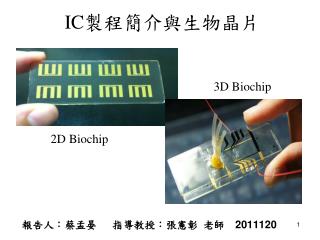
報告人:蔡孟晏 指導教授:張憲彰 老師 2011120. IC 製程簡介與生物晶片. 3D Biochip. 2D Biochip. Outline. 1. 生物晶片 (Biochip). Evaporation. PVD. Sputtering. 2. 薄膜 沉積. CVD. 製程部分簡介. APCVD. LPCVD. PECVD. Wet etching. Dry etching. RIE. 3. 蝕刻. Biochip ( 生物晶片 ). 傳統上,在實驗室檢測生物樣本大多需要眾多儀器與專業知識才能進行檢測。

IC 製程簡介與生物晶片
E N D
Presentation Transcript
報告人:蔡孟晏 指導教授:張憲彰 老師2011120 IC製程簡介與生物晶片 3DBiochip 2DBiochip
Outline 1. 生物晶片(Biochip) Evaporation PVD Sputtering 2.薄膜 沉積 CVD 製程部分簡介 APCVD LPCVD PECVD Wet etching Dry etching RIE 3.蝕刻
Biochip (生物晶片) • 傳統上,在實驗室檢測生物樣本大多需要眾多儀器與專業知識才能進行檢測。 • 近十幾年由於製程技術的進步,將微機電製程(Micro electric Mechanical System, MEMS)運用於檢測上因而誕生了生物晶片。 • 生物晶片大多運用電動力學原理於濃縮、分離、捕捉、集中樣本。
晶片製作過程 清洗 蒸鍍 以丙酮、異丙醇清洗玻片上的油脂、有機物質 載玻片 蒸鍍上金和鈦的載玻片 曝光、蝕刻 定義電極圖形
Outline 1. 生物晶片(Biochip) Evaporation PVD Sputtering 2.薄膜 沉積 CVD 製程部分簡介 APCVD LPCVD PECVD Wet etching Dry etching RIE 3.蝕刻
Thin films Deposition Physical Vapor Deposition (PVD) (1) Evaporation Thermal (2) E-beam evaporation (3) Sputtering Chemical Vapor Deposition (CVD) (1) Atmospheric pressure CVD (APCVD) (2) Low pressure CVD (LPCVD) (3) Plasma enhanced CVD (PECVD) http://python.rice.edu/~arb/Courses/chem360_06.htm
Aluminum Power supply To pump Thermal Evaporator • This can be reached only under high vacuum conditions: pressure of <1 mPa • Consequently expensive pumping systems and long pumping times are needed . • The distance between evaporator and the substrates has to be comparable with free path for evaporated atoms.
Power supply To pump Electron Beam Evaporator • Electrons are emitted from the resistively heated filament and accelerated between the filament and accelerating grid. • Electrostatic deflection plates control the e-beam position • Strong magnets generate magnetic field causing 270º bending of the e-beam • E-beam can be restored across the charge to melt a significant fraction of the surface. • Crucible (坩堝) is water-cooled to reduce the contamination • Many crucibles for compounds • Problem for semiconductors: radiation damage (UV, X-ray) electron beam
Evaporator Electron BeamEvaporator Thermal Evaporator
Radio frequency (RF) is a rate of oscillation in the range of about 30 kHz to 300 GHz Sputtering (濺鍍) • The major PVD method in silicon technology • Using ion bombardment to introduce mass transfer • Low temperature process can deposit virtually any materials, contain metals, ceramics, organic. • Can deposit composite film (alloy) with controllable composition. • Major disadvantage: substrate damage DC sputtering RF sputtering Magnetron sputtering
晶片製作過程 清洗 蒸鍍 • 本實驗室的生物晶片是使用電子束蒸鍍(Electron Beam Evaporator)在載玻片上進行鈦與金的物理性薄膜沉積。 • 薄膜沉積是先鍍上鈦隨後才是金,這是因為金無法與載玻片有良好的貼附性才使用鈦當作金與載玻片之間的介質。 以丙酮、異丙醇清洗玻片上的油脂、有機物質 載玻片 蒸鍍上金和鈦的載玻片 曝光、蝕刻 定義電極圖形
Outline 1. 生物晶片(Biochip) Evaporation PVD Sputtering 2.薄膜 沉積 CVD 製程部分簡介 APCVD LPCVD PECVD Wet etching Dry etching RIE 3.蝕刻
Chemical Vapor Deposition (CVD) Chemical vapor deposition (CVD) forms a thin film on the surface of a substrate by thermal decomposition and/or reaction of precursor molecules (gaseous compounds) Al in TiN 265℃ 1. Vaporization and transport of precursor molecules into a reactor. 2. Diffusion of precursor molecules to the surface of the substrate. 3. Adsorption of precursor molecules to the surface and further diffusion across the surface. 4. Decomposition of precursor molecules and incorporation into solid films. 5. Desorption of volatile byproducts into the gas phase. Slowest Step Dominates • Reaction-rate limited process • Mass-transport limited process Silicon : SiH4(g)→Si (s) + 2H2(g) Silicon dioxide: SiH4(g) + O2→SiO2(s) + 2H2(g) Silicon Nitride: 3SiH4 + 4NH3→Si3N4 + 12 H2 Tungsten: WF6→ W +3F2
Atmospheric CVD (APCVD) gas gas SiO2 deposition SiH4 (g)+O2 (g) →SiO2 (s)+2H2 (g) • High deposition rate • Poor uniformity, high contamination level. • Operation temperature 500~800°C • Application for dielectrics(SiO2, Si3N4)
Low Pressure CVD (LPCVD) TEOS oxide at 700°C • Low pressure: from 0.1 to 1 Torr • Used mainly for polysilicon, silicon dioxide and silicon nitride films. • • Can process 200 wafers per batch. • Typically performed temperature in 300~900 °C • Allows chemical deposition of thin film with the best quality
Plasma Enhanced CVD (PECVD) PECVD TEOS Si(OC2H5) + O2 → SiO2+ byproduct Tetraethyl Orthosilicate (TEOS) 四乙基正矽酸鹽 • High deposition rate at relatively low temp (20~150°C) • • RF induces plasma field in deposition gas • Developed for silicon nitride and silicon dioxide
Outline 1. 生物晶片(Biochip) Evaporation PVD Sputtering 2.薄膜 沉積 CVD 製程部分簡介 APCVD LPCVD PECVD Wet etching Dry etching RIE 3.蝕刻
Etching • Film an area define by lithographic step removed or etched away. • Etching type: wet etching and dry etch.
Etching Process • Anisotropic: - best for making small gaps and vertical sidewalls - typically more costly • Isotropic : - quick, easy, cheap. - best to use with large geometries, when sidewall slope does not matter, undercut/release. - rounding of sharp anisotropic corners
Wet Etching • What is wet etching? - material removal reaction occur in the liquid . • Mixtures of acids, bases, and water - HF, H3PO4, H2SO4, KOH, TMAH, H2O2, HCl, .. • Can be used to etch many materials - Si, SiO2, Si3N4, PR, Al, Au, Cu,… • Etch Rate: - wide range • Etch Selectivity - typically quite high - sensitive to contamination • Etch Geometry • typically isotropic, some special cases are anisotropic.
Wet Etching Advantages: • Low cost • Orientation dependant • Controllable etch rates • High selective Disadvantages: • Contamination • Dangerous • Etch rate varied by temperature and concentration
晶片製作過程 • 本實驗室的生物晶片是以濕式蝕刻,經沉積不同物質與不同沉積厚度,所使用的化學藥劑與浸泡時間都會有所改變。 • 我們的晶片是沉積金與鈦,所使用的化學藥劑分別為金蝕刻液與鈦蝕刻液。 • 在金的蝕刻時間上大約浸泡45秒。 • 在鈦的蝕刻時間上大約浸泡5秒,蝕刻液需加熱至90度。 清洗 蒸鍍 以丙酮、異丙醇清洗玻片上的油脂、有機物質 載玻片 蒸鍍上金和鈦的載玻片 曝光、蝕刻 定義電極圖形
Dry Etching What is dry etching? • material removal reaction occur in the gas phase Type of dry etching • non-plasma based dry etching • Plasma based dry etching Advantages: • Directional etching without using the crystal orientation of Si • High resolution • Ease of automation Disadvantages: • Some gases are quite toxic and corrosive • Re-deposition of non-volatile compounds • Need of specialized (expensive) equipment
Method of Dry Etching • Physical etching:(e.g. sputtering etch), mechanical/physical interaction. • Chemical etching: - neutral or/and ionized species interact with the material’s surface to form volatile products • Combinations of Chemical and Physical Etching - Anisotropic profile, reasonably good selectivity, and moderate bombardment-induced damage
RF plasma based dry etching CF4 + e﹣→ CF3 + F +2e﹣ F + SiO2 → SiF4 + O F + Si3N4 → SiF4 + N • low dc bias is generated • the energy of bombarding ions is not sufficient to sputter the substrate • chemical species are produced in plasma • removal of substrate materials occurs due to chemistry • substrates are placed on the grounded electrode
photoresist photoresist ion Etch byproduct Atom Free radicals Reactive ion Etching (RIE) • Chemically reactive plasma is generated • Cathode is biased with RF power • Cathode is smaller than the anode dc bias of few hundred of volts is induced on the cathode • Positive ions are accelerated across the plasma sheath • Removal of material is by both sputtering and chemistry
Summary • 生物晶片在檢測技術上有著跨時代的進步,於實驗室眾多儀器的分析處理改進至一片微小的生物晶片上。有體積微小的優點,還有所需檢測樣本少、檢測時間短、成本低廉。 • 薄膜沉積技術在著重材料研發改質的時代裡地位就更顯重要,未來的世界裡,人類的生活中舉如工業、生醫領域,將因薄膜技術的應用而獲得更多的進步,同時在講究環保的今日,PVD的薄膜沉積技術應會被列為技術研發的首要考量。 • 蝕刻技術中,乾式蝕刻因具有高度非等向性蝕刻能力,應用於IC或MEMS的系統製程上有著不可取代的地位,尤其高深寬比的製程技術,將在奈米結構的發展上產生極大的應用。