Download

1 / 32
400 likes | 610 Views
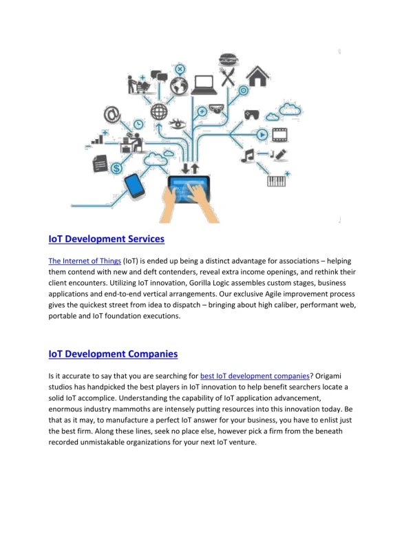
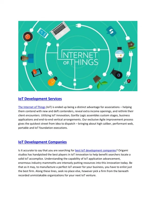
Product Engineering Company- IoT, Semiconductor & Systems. MosChip is Product Development company with over 16 years of extensive expertise in semiconductor / systems / IoT engineering from SoC (Systems on Chip), Embedded Systems Design, Cloud and Mobile Software development catering to the Aerospace & Defence, Consumer Electronics, Automotive, Medical, Telecommunications, Mobile industries. <br>With over 400 Clients in 140 countries, Moschip has also put its footprint in the field of IoT, Cloud and Connected Devices domain. Driven by a positive outlook, Moschip is moving to more flexible, agile models.<br><br>https://moschip.com<br>

E N D
Over view MosChip is a complete Product Development company with deep engineering expertise in Chip Design, Systems Design, Software development for IOT & Vision solutions. We have 16+ years of proven track record with unique combination of product engineering skills, domain knowledge and technology expertise in segments such as aerospace and defense, consumer electronics, networking and telecommunications, mobile electronics and security etc. We help our customers to reduce time–to-market of their products with our field proven IP’s. Our product development experience with SOC, wireless connectivity, software, and systems engineering allows us to be able to meet even the most complex hardware and software design challenges. With a large pool of engineers segmented into teams with multiple engineering disciplines, MosChip can deliver ASIC, firmware, drivers, boards, and platform solutions
Awards & Recognition Winner of “BEST PRODUCT DESIGN COMPANY IN A&D” at DEFTRONICS awards 2016 3
Our Journey Emerged as a strong players in IoT Additional $10m funding by Promoters Listed on BSE in 2001 Key Defense Projects awarded April 2016 Founded in 2000 Acquisition of Elite Plus, Orange, Maven (IoT) & Next Generation(Board) Development 20 different products in Connectivity from inception Acquisition of controlling stake by Techwave 2016 YTD MosChip valuation Growth 15x Sold 10m+ chips to customer such as Toshiba, Sony, IBM more Developed SOC MCS8142 in 2010
Locations Maidenhead (UK) Milpitas (USA) Hyderabad (HQ) IND Pune Bengaluru Singapore Project and Sales Offices Design Centre, Project and Sales Office
Service & Offerings Turnkey solutions Provider Semiconductor Development IP Development for Vision Processing & Deep Learning Internet of Things IoT Enablement MOSCHIP “A Solution Company” Engineering Service W / Strategic Customer Engagement System & FPGA Platform Solutions
Why MosChip ? Multi-Disciplined Team Turnkey Solutions Innovation Driven Customer First With 16+ years of successful track record MosChip provides a unique combination of product development expertise ranging from Chip Design to Systems Development. Our customer driven approach focuses on all facets of the product development process, including not only technology, but also time-to-market and return on investment. MosChip keeps up to its clients’ vision by developing their next generation flagship product lines, that are key and rare in the industry. We have a large pool of engineers segmented into teams with multiple engineering disciplines namely ASIC, firmware, drivers, boards, & platform solutions.
Product Development Lifecycle • Design Consulting • Product Planning • Product Development • Post Market Support
SoC Design Expertise • We will provide solution from Specification to GDSII • Fully equipped to take end-to-end design services activities Turnkey solutions Provider With Partners DESIGN VERIFICATION POST SILICON FABRICATION/PACKAGING Verification Planning Specification Timing DFT Architecture Architecture Fabrication Test Assembly/ Packaging Post Silicon Services Evaluation/Board Testing IP Verification RTL Coding Layout Soc Verification Synthesis Synthesis
SoC Design Service (Providing services from Concept to Silicon) Experience Summary Key Differentiators • Unique combination of Silicon & Systems • Product development experience • Outstanding Processes, templates, structures & • checklist for scaling up • Robust Internal Design Flows • Low Power Design Expertise • In-house developed reusable Cores (USB2.0 & 3.0) • Early adopters of advanced ASIC Verification methodologies • like VMM, OVM & UVM. • Developed Scalable, Configurable, & Reusable • Verification test bench • Large Designs Exposure • Analog/Mixed Signal Expertise • Power Optimization Experience • Yield Enhancement Services • 20+ ASIC Tape outs • First Pass Silicon Achievement • 100% On-Time Delivery • FPGA to ASIC Translation • 40nm TSMCLP Design • 28nm TSMCLP verification • 55mn gate density largest design
Case Study : Shikhara Soc (Targeted For TSMC 40nm Low Power ) • ASIC Development For Shikhara SoC • Specifications to Silicon • System Integration, Synthesis and Verification. • Verification environment development using C, • Assembly and VMM/UVM. • The debug and Trace Capability to cover entire SoC. • Perform Power aware DFT and ATPG generation. • Development of FPGA platform for system level verification. • Physical design and verification. • Development of Load Board and Test Software • (To Test SoC on ATE). • Wafer Fabrication, packaging, assembly and testing • (Using CMOS 40nm LP). • Development of Evaluation board and board support package • Firmware Development • iBoot (Internal Boot Code Development). • UBoot Boot loader development. • Development of controller drivers • Linux BSP development. • Linux Root file system development • Development of Test Applications to validate BT, Video, GPU, Camera and Display subsystem. • Developed Shikhara architecture, design document for controller driver, etc. • Shikhara SoC Features: • ARM cortex A9 dual core processor • with NEON VFPU • Trust Zone Support for ARM. • ADB400 for Power Management. • ARC processor based AV417 Video Subsystem • & Bluetooth Subsystem. • MALI-400 - OPEN GL 2.0 & OPEN VG 1.1 GPU • Over 250Million Transistors
Case Study High Definition Camera SoC Verification H . 264 encoder, RGMII, SDMMC / SDIO, USB2.0 OTG, GPIO, SPI, PWM, 12C, 12S, UART Understand IP Specification & Design Architecture Documents Verification Architecture & Test plan Documents Prepare Verification Environment Documents Customer: US Based Company Verification of H.264 IP High Definition Camera SoC Services / Solution: System Verilog & C Language: Tensilica 233L, Tensilica 330HiFi Processors: IUS9.2 Tools Implementation of Verification Architecture & Test Cases (in SV & .C) Implementation Fictional Verification Sign – off on RTL Execution & Start us Report DUT (IP & SoC)
Case Study High Definition Camera SoC Verification Business Need • H.264 Encoder IP and SoC verification using System Verilog and C • H.264 Encoder IP Verification • Verification environment development using System Verilog • Verification IPs development and test cases implementation in System Verilog • Coverage-driven and Constrained-Random Verification • Code and functional coverage analysis • SoC Verification • Verification environment development for all the peripherals in System Verilog. • Implementation of test cases in C. Automate the verification environment using PERL Scripting. • H.264 IP and SoC RTL verification sign off Scope • Adhering strict timelines to ensure time to market. • Target to achieve 100% functional and code coverage on H.264 IP verification. Challenges • Developed reusable verification environment for all the peripherals which • can be ported on IP and SoC • H.264 IP validated thoroughly at IP level which reduced verification • time at system level. • Multiple teams working in parallel at different geographical locations to speed up the project • execution and to reduce the cost. Business Benefits
System/Board Design Services (Leveraging product development to custom engineering services) System Design Board Design Capabilities • Expertise in Multilayer Complex board designs • Rich experience in High Speed Mixed signal designs • (Analog, Digital & RF) • Schematic Capturing & Component Library creation • Signal & Power Integrity • Reengineering • High first time success rate • Component Assembly • Board bring up and testing • System Debug • PCB Designs of up-to 24 layers • 250+ System designs of varied complexity • High Density Interconnect (HDI) designs • Handling 0.8mm pitch BGAs • Design using Buried & Blind vias • Impedance controlled and high speed designs • Signal Integrity, Power Integrity & Thermal Analysis • Dedicated resources for Schematic design, PCB design / Signal Integrity, Component assembly & Testing • Full support PCB Manufacturing, components Assembly and equipment • EDA Tools : Cadence & Mentor Graphics For • Schematic Capture, PCB layout • Signal Integrity, Power Integrity & Thermal Analysis
System Engineering Domain Expertise FPGA Design Capabilities • High Density FPGA based design • Soft Processor Integration • IP Development & Integration • Reference Design Development • RTL Design & Synthesis • Verification & Validation • Hardware/Software Partitioning • Test bench Generation • Low power designs • ASIC Prototyping • Handling of High-end FPGAs • Xilinx: Virtex-II Pro, Virtex-4/5/6, Virtex-7, Spartan, ARTIX, ZYNQ • Altera: Cyclone-II/III, Stratix-III/IV • FPGA Families - Xilinx & Altera Series • Single and Multi Clock Domain Logic • Frequencies up to 500MHz • PLL, DLL an DCM • Soft Processor - ARM, NIOS, MicroBlaze & Power PC • Processor interfaces - AMBA AXI, AHB, APB, VCI, etc. • Bus Interfaces • USB 2.0/3.0, OTG, PCIe Gen 1/2/3, PCI, ISA, • Ethernet(10/100/1000), TCP offload Engines • RGMII, MII SATA, PATA, SDIO, FireWire, IrDA, CAN, I2C, SPI, … • Audio/Video Interfaces - Codecs AC97, I2S, CSI, LVDS, Video ADC & DAC, HDMI, LCD, DSI, BT656, • Memory interfaces • SDRAM, DDR/2/3, LPDDR • Flash (SPI & Parallel) CFD, SD Card, MMC … • Wireless - WIFI 802.11 b/g/n, ZigBee, Bluetooth • Voltage Levels - LVPECL, LVDS, LVCMOS, LVTTL • Operating voltages • 1v to 5v • Storage Security: IEEE-P1619 compliant XTS-AES
Embedded Software Services... Platform Development (BSP) Embedded Software • ASSP SW Development, Board Support Packages • Boot loaders, OS/ Kernel Bring up, Porting • Linux, VxWorks • Android, Windows • Device Drivers • DMA, I2C, I2S, McBSP, UART (HS/FS) • MMC/SD, SPI, eMMC, SDIO • Touch Screen, LCD/LVDS • NAND, NOR • A/V, HDMI, MIPI DSI/CSI • USB, WLAN, IrDA • Ethernet, BT, PCI, PCIe • Multimedia (Audio, Video) • Power on Diagnostic, Power management • Multi-Media Framework Dev & Porting • OS Porting & Board Support Package (BSP) • Device Drivers – Bare metal, OS • ARM, freeScale, TI, Samsung, Qualcomm • Multimedia Middleware Components • Display/Video/Audio controllers • Audio/Video CODECs • 3rd Party IP, Application Integration • System Integration & Validation • Benchmark, Compliance Testing • Product Development / Customization
Testing Expertise… Testing Expertise Summary Types of Testing Areas of Testing Expertise Test Automation • System integration and • validation • BSP Validation • Benchmark testing • Functional Testing • Performance Testing • Load/Stress Testing • Reliability testing • Compliance Testing • Compatibility Testing • Interoperability Testing • Integration & Regression • Testing • UI Testing • Environmental Stress Testing • Creation of Test Strategy • Creating Test Plan • Test Case Design • Prepare and maintain Test Coverage/Specification documents • Test Case Execution • Defect Identification, Analysis & Fixing • Communication written/oral • Defect reporting & tracking • Detailed Test Summary report creation • Covering silicon, systems, embedded software and OS • Automation Framework Development • Test Suite Automation using • C • Shell Scripting • Perl Scripting • Python Scripting • Areas • Software Device Drivers Testing • Embedded Application Testing • Connectivity Testing • PCI/PCIe, Ethernet/ Serial / Parallel / USB/I2C /SPI/I2S • Network Testing • Network Protocols (TCP/IP Suite, Wi-Fi, ZigBee, Bluetooth), • Storage Testing • Testing of Storage Controllers like (SATA, NAND etc.) • Consumer Network Storage solutions like NAS, iSCSI, AoE etc.) • POS, Digital Signage etc.
Shikhara FPGA Platform (One Virtex – 7 FPGA & One ZYNQ – 7045 SoC) • Key PCB Information : • Board Size: 11” x 12” • Layer Count : 16-Layered • Component Count: 2388 • Signal Nets Count: 8929 • Virtex-7 FPGA pin Count # 1925 • ZYNQ-7045 SoC pin Count# 900 • Operating Frequency: • Memory @1.067GT per second • GTX links @6.25Gbps • USB3.0 PIPE: 16bit@250MHz • Critical Interfaces: • DDR3 SDRAM, USB3.0 • Gigabit Ethernet, GTX-Serial Link Interface • SMC, CSI-DSI, HDMI, AUDIO • High-Speed SI SAMTEC connectors • Wireless Supported: • Bluetooth • GPS/GNSS
Case Study - Face Recognition System (Based on CAM LINK Data - Appliance Processor) • Key PCB Information : • Board Size: 216 x 215 mm • Layer Count: 16 – Layered • Component Count: 1706 • Signal Nets Count: 1265 • 2# Virtex - 6 FPGA pin Count: 1156 • 1# Virtex - 5 FPGA Pin Count: 1738 RECONFIGURABLE FACE RECOGNITION PLATFORM • Operating Freq: • CAMLINK LVDS: 2GHz • GTX link: 3.125GHz • Critical Interfaces: • DDR3 SDRAM • USB2.0 Host • Gigabit Ethernet • GTX – Serial Link Interface • CAMLINK 26-pin Miniature Delta Ribbon connector (MDR-26)
Case Study - OCTOPUS (Common Processor Board & Chassis)
Vision Related Core Competency and building more… Expertise in Camera Domain Algorithm, Architecture, Camera Domain Expertise • Advanced algorithms implemented • Silicon & software architecture delivered • Multiple markets addressed: activity; • surveillance; DSLR/DSMC; embedded Multiple Generations of Products Delivered in Previous Companies Delivered Multiple Generations of Imaging & Video Solutions • Delivered volume prod to mobile, activity, • surveillance, dental and others • Developed roadmap for products, • multiple generations outlook Engaged with Major Customers From Concept to Production Tremendous Customer History, Market Engagements • Standard products delivered to customers • around the world • Custom product with strategic partner 21
IoT & Services... End to End Offering Custom Devices & Systems Scalable Cloud Platform Value Added Software & Services Hardware Boards & Modules Vertical Application Solutions From Sensor Network Collect & aggregate data in gateways & Smartphones Smartphone apps, alerts , Data Analytics IoT / M2M Platforms Ready for Connecting Large Numbers of Nodes
IoT & Services... M2M / IoT “ enablers & accelerators” Application Specific Reporting & Data Analysis Alerting Alarming Mechanism Remote over-the-air Firmware Upgrade Remote Diagnostics & Health Check Remote Configuration Quickly Customize Solutions For New Domains Reduced Time to Market Using the M2M / IoT Accelerators ! IoT Node WNS = Wireless Sensor Node Real – Time Data Transfer + Storage WSN WSN WSN M2M Node DCU / Gateway Cloud Connectivity (Cellular / WiFi / Ethernet Cloud Connectivity (Cellular / WiFi / Ethernet (Zigbee / WiFi / BT Sub 1GHz Mesh) Application Specification Intelligence Application Specification Intelligence Application Specification Node Intelligence Local Data Handler & Storage Local Data Handler & Storage Local Data Handler & Storage Sensor/Actuator Interface Sensor/Actuator Interface Device Protocol Interface Device Protocol Interface WSN (Zigbee / WiFi / BT Sub 1 GHz Mesh)
IoT Solutions Offering School buses Heavy equipment Solar/wind mills Sub metering Street lighting Diesel generators Township automation Commercial vehicles Commercial lighting Offshore platforms Employee buses /cabs Sales force monitoring Underground mining Residential metering
Remote Monitoring Solutions Smart Metering Solutions Vehicle Monitoring Smart Lighting Solutions Diesel Generator Monitoring Asset Monitoring Wearable Devices 25
Market Verticals Covered Semiconductor Security Surveillance & Access Control Aerospace & Defense IoT, Cloud & Connected Devices Retail Transport & Logistic Medical Devices Home & Industrial Automation Consumer Electronics Network & Telecom Automation Medical Communication
Engineering Team ASIC/FPGA (83 Engineers) SOFTWERE (48 Engineers) Design, Verification, Synthesis & STA BSP, Linux, Driver development & Testing INDIA : 248 USA : 18 Total : 276 ENGINEERS UK / EUROPE : 10 Board Design, Layout Testing (58 Engineers) IoT & platform (60 Engineers) Design, Layout & Testing Design, Software & Support
MosChip EDA & Languages EDA Tools Expertise (Development & Testing) • Cadence IUS • Synopsys VCS-MX, MVSIM, MVRC • Synopsis–DC for synthesis, Prime Time for STA • Surelint by Verisity for Linting • Cadence-ICCR – Code coverage • Cadence simulator – NcVerilog • Xilinx ISE for FPGA validation • Synplicity for FPGA Synthesis • Xilinx Vivado • Altera Quartus for FPGA synthesis • ARM tools – DS5, DSTREAM etc. • Verilog, System Verilog & VHDL • Shell, PERL, PYTHON & TCL Scripting
Why MosChip? • Unique Combination of Silicon and Systems • Product Development Experience • Outstanding Process, Structures and checklist for scaling up • We uniquely combine business dynamics with technology, very few companies have this combination • Grown up with the methodologies • Pioneered and deployed several traditional and advanced Digital, MS and LP methodologies. • Several years of hands on experience in developing modular based traditional and advanced verification environments. • Developed and Integrated several Verification IPs – elite + engineers know what takes to develop a good VIP, which integrates smoothly into the Verification environment. • Proven Track Record in.. • Deploying several these methodologies in industry leading companies. • Claimed several FIRST-PASS verification success. • Trusted verification eyes to develop your standards, protocols, and test infrastructures, • whilst product companies focus on their designs and development. • Cost effective and High Quality Engineering Services. • Go-to centre of excellence where results really matter.
Official Locations INDIA Pune "Govind", 7 C Shri Ganesh krupa society S No 91/1, Kothrud, Off Paud road, Pune 411038 Ph: +91 20 2539 6775 Fax: + 91 20 2539 6775 Bangalore (at Koramangala) 13/36, 3rd cross, Venkatareddy Layout, 80 Feet road, Koramangala, Bangalore - 560095 Ph: +91 80 41603939 Fax: +91 80 41603939 Hyderabad (Headquarters) Plot # 83 & 84 Punnaiah Plaza, 2nd Floor Banjara Hills Hyderabad – 500034Tel: +91-40-6622-9242Fax: +91-40-6622-9393 Bangalore (at HSR Layout) 991 & 992, 2nd floor, 5th main, 7th sector, HSR Layout,Bangalore – 560 102 Tel: +91 80 25722427 Fax: +91 80 25722427 USA UK www.moschip.com Milpitas840 N. Hillview Drive Milpitas California 95035Tel: 408-737-7141Fax: (408) 737-7708 Maidenhead4 Havelock Road Maidenhead UK SL65BJTel: +44 (0) 3301137863Fax: +44 (0) 3301137863 Moschip Semiconductor Technology Ltd MosChip-Semiconductor