Download
1 / 4

E N D
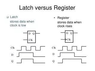
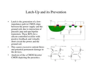
Latch is the generation of a low-impedance path in CMOS chips between the power supply and the ground rails due to interaction of parasitic pnp and npn bipolar transistors. These BJTs for a silicon-controlled rectifier with positive feedback and virtually short circuit the power and the ground rail. This causes excessive current flows and potential permanent damage to the devices. Analysis of the a CMOS Inverter CMOS depicting the parasitics. Latch-Up and its Prevention
The equivalent circuit shown has Q1 being a vertical double emmitter pnp transistor whose base is formed by the n-well with a high base to collector current gain (b1). Q2 is a lateral double emitter npn transistor whose base is formed by the p-type substrate. Rwell represents the parasitic resistance in the n-well structure whose value ranges from 1KW to 20kW. The substrate resistance Rsub depends on the substrate structure. Assume the Rwell and Rsub are significantly large so that they cause open circuit connections, this results in low current gains and the currents would be reverse leakage currents for both the npn and pnp transistors. If some external disturbance occurs, causing the collector current of one of the parasitic transistors to increase, the resulting feedback loop causes the current perturbation to be multiplied by b1.b2 Latch-Up Continued
This event triggers the silicon-controlled rectifier and each transistor drives the other with positive feedback eventually creating and sustaining a low impedance path between power and the ground rails resulting in latch-up. For this condition if b1 *b1 is greater than or equal to 1 both transistors will continue to conduct saturation currents even after the triggering perturbation is no longer available. Some causes for latch-up are: Slewing of VDD during start-up causing enough displacement currents due to well junction capacitance in the substrate and well. Large currents in the parasitic silicon-controlled rectifier in CMOS chips can occur when the input or output signal swings either far beyond the VDD level or far below VSS level, injecting a triggering current. Impedance mismatches in transmission lines can cause such disturbances in high speed circuits. Electrostatic Discharge stress can cause latch-up by injecting minority carriers from the clamping device in the protection circuit into either the substrate or the well. Sudden transient in power or ground buses may cause latch-up. Latch-up Continued
Reduce the BJT gains by lowering the minority carrier lifetime through Gold doping of the substrate (solution might cause excessive leakage currents). Use p+ guardband rings connected to ground around nMOS transistors and n+ guard rings connected to VDD around pMOS transistors to reduce Rw and Rsub and to capture injected minority carriers before they reach the base of the parasitic BJT. Place substrate and well contacts as close as possible to the source connections of the MOS transistors to reduce the values of Rw and Rsub. (solution to be used in your designs) Place source diffusion regions for the pMOS transistors so that they lie along equipotentials lines when currents flow between VDD and p-wells. Avoid forward biasing of the source/drain junctions so as not to inject high currents , this solution calls for the use of slightly doped epitaxial layer on top of the heanily doped substrate and has the effect of shunting the lateral currents from the vertical transistor through the low resistance substrate. Guidelines For Avoiding Latch-Up