Download
1 / 13
130 likes | 304 Views
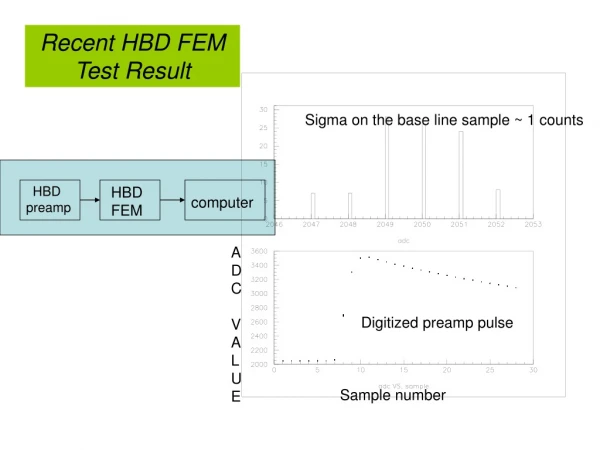
HBD FEM. Overall block diagram Individual building blocks Outlook ¼ detector build. FEM Block diagram. Connector. 8 Channels 65 MHz 12 bits ADC. FPGA Receive/buffer ADC data Format triggered Events Generate L1 Primitives Receive timing /clocks. Signal cable.

E N D
HBD FEM • Overall block diagram • Individual building blocks • Outlook • ¼ detector build.
FEM Block diagram Connector 8 Channels 65 MHz 12 bits ADC FPGA Receive/buffer ADC data Format triggered Events Generate L1 Primitives Receive timing /clocks Signal cable Differential Receiver Data path L1 primitive
Cable (connector) choiceBefore Oct 2004 3M shield twist pair cable 1785/34 (17 pair 16 signal + grounds) connector 3431 size = 62.6mm + 9.4mm(ejector) 80 signals => 36 cm 3M MDR (Mini D Ribbon) cables Need to have custom build 50 pins cable example 14150-ezbb-xxx-0lc connector 40 position 10226-1210 VE 47.1mm for 16 pairs 235.5 mm for 80pairs. 25mm for power and test pulse. Detector has 8 panels Readout both side of the panel Panel size 23x26 cm
The Current Cable Choice We would use the infiniband 12X cable It has 24 individually shielded differential parallel pairs 48.9mm wide for cable/connector end 0.5mm between signals/grounds For 26awg cable 3.2“ bending radius (cable OD: 0.540") Assembly 90-Degree Bend Radii is 5.7” for 26 awg. 1.5mm Caution: connector is made of zinc cast. cable are heavy we need to use vertical daughter card to bring the signal out
The differential receiver Use Analog Device AD8138 receiver set up as unity gain Simulation result For 16fc input charge Total voltage On the cable ADC has 1V range Max ADC range is about 7~8 time of 16fc Total voltage Seen by ADC ADC +/- inputs
The 8 channel 12 bits 65MHzADC The ADC receives differential signals The Vcommon is 1.5V The +/- input can swing from 1V to 2V + side 2V, - side 1V -> highest count - side 2V, + side 1V -> lowest count Our +/- input will swing from 1.5 to 2V/ 1 to 1.5V we will only get 11 bits out of 12 bits 16fc will be roughly sitting 256 count We will run the ADC at 6X beam crossing clock 6X9.4 MHz = 56.4 MHz or ~17.7ns per samples
FEM BOARD We layout the differential receiver block An layout example file was send to the assembler to comment on… O.K. Currently we can pack receiver in 8 mm pitch We will set FEM card to be a 6U module 48 channels per card Receiver will be layout to be 2 rows. Each row will have 24 receiver blocks. With 96 channels per panel per side total channel count is 1536. It will fit in two 6U VME styles crates. ~ 5 cm
FPGA • Receive ADC data, provide L1 delay, Multiple L1 triggered events, format data, generating L1 trigger primitives, manage clocks, test pattern etc. • 48 channel of serial ADC => 48 *720 Mbits/sec or 34 Gbits/sec need to be received. • We choice Altera Stratix EP1S30 1020 pins package as the device for 32 channels before we change the cables. • We need to re-evaluate which FPGA device we will use… • Otherwise we will pay higher cost per channel… • (either one larger FPGA for 48 channels of data or smaller one for 24 channels of data)
HBD data to DCM • 12 samples per channel • Cover 2 beam crossing • Assume the optical will run 6X beam crossing rate. • 24 channel will take ~16.6 ns*24*12=4.8 microsec • We will merge 4 24 channels sets of data into one optical links in un-multiplexed mode • 8 24 channels sets in multiplexed mode to DCM
Trigger data • Each channel has 7 of threshold -> 3 bits • Link run at 6x beam crossing rate. • every clock cycle can send 4 channel of data (12 bits), 24 channel of data for every beam crossing.
Outlook • If there are no more changes, We still looking at 5 months before we can have the any prototype modules. • The test will probably finish 3 months after that, if there is no major errors. • The Production will take 6-9 months.
Logistic issue in the ¼ detector readout • If we can pack 48 channel into the FEM, we will have 32+4 FEM, 2+2 backplanes, 2+2 crate interfaces and 2+2 crates. This is a small build. • The printed circuit board manufactures have minimum lot charge, we are very close to it. Splitting the PCB order will double the cost. • We will order 40(80) FPGA, 200+ ADC for the whole build. Splitting order will just increase the overall cost. • The assembler has setup charge. We will pay the setup charge twice when splitting the order. • We will need to increase the EDIA cost in Nevis because we need to repeat the construction process twice, i.e. order, prepare the assembly kits etc…
Possible Solution • Increase the prototype module number from 2(3) to 10(11). • Don’t assemble the board till the first two boards is working. (still has to pay the additional setup charge) • We will look at 5-10% increase in the overall budget in this scenario. • We will need the money in few months to buy the additional compoents.