Download
1 / 32
320 likes | 462 Views
Mixed Analog and Digital Circuit Boards for the ATLAS TRT. Nandor Dressnandt, Godwin Mayers, Toni Munar, Mitch Newcomer, Rick Van Berg, Brig Williams University of Pennsylvania Bjorn Lundberg Lund University Thurston Chandler, Colin Gay Yale Curt Baxter University of Indiana.

E N D
Mixed Analog and Digital Circuit Boards for the ATLAS TRT Nandor Dressnandt, Godwin Mayers, Toni Munar, Mitch Newcomer, Rick Van Berg, Brig Williams University of Pennsylvania Bjorn Lundberg Lund University Thurston Chandler, Colin Gay Yale Curt Baxter University of Indiana
End Cap Wheel Barrel Electronics Readout on Tread Barrel Readout in 2.5cm Crack TRT Physical Layout 325,000 Wires 104,000 Wires NSS 2003
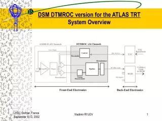
Full Readout With Custom ASICS LVDS (like) Clock/Control/Data Chip to Back End Low Level Differential Ternary Output (200uAStep) ASDBLRDTMROC 16 Channel Readout ASIC Triplet NSS 2003
Barrel TRT Module End Barrel Support Frame HV Connector Arrays of 16 Straw Wire Anodes + 6 (AC coupled) Cathode Ref Straw wire Density 30mm2/ straw 2X the density of Wheel NSS 2003
40MHz Logic Stamp Board Approach 16 Channel ASIC triplet Readout Stamp FLEX Boards KaptonConnection Output Roof Connector DTMROC in TQFP Chip on Board ASDBLR’s Low Manufacturing Yield Sensitive Analog Inputs Cathode Reference Inputs from straw wires NSS 2003
ASIC Packaging Custom Fine Pitch Ball Grid Arrays 16 Channel DTMROC 11X13mm ASDBLR 8channel ASDBLR 8channel 7.2 X 9.6mm NSS 2003
Stamp Board Threshold Scans Large Channel to Channel Variations due to Clock pickup # Hits in 75ns Gate Increasing Thresold NSS 2003
Other Conductors Cable Shield currents, Dgnd bounce noise Signal Return Path External currents added in signal return path can seriously corrupt straw signal. Ideal Signal Return ASD Preamp Agnd Connector pins Straw reference Plane HV CAP Straw Cathode These currents may be redirected over a large area by adding a low impedance network of conductors at the end of the module. NSS 2003
Single Analog and Digital Board Approach Module 1 Small Triangle (one of 16 Custom Barrel Designs) Data Cable Connector (Unstuffed) Top Side Digital Access along All Edges to Analog GND Encloses Detector Ends DTMROC ASICS Power Under side Analog Straw Pin Floating Contact (NAIS) Connector Input Protection Board(s) 16 Straw modularity 1 of 10 Boards Shown ASDBLR ASICS underside NSS 2003
First try at A and D Board • Hopeful but not very good. • Clock pickup between supplies. • Poor access to board grounds at the top of the board. • Line over line differential clock / control routing near inputs. • Trial areas where different routing techniques were studied. • It did provide an essential case study to justify effects of various design • techniques that otherwise would be simple speculation. Motivates Common Sense Design Rules: • Separate Analog and Digital Power Domains. • Maximize distance between Digital and layers and Analog power layers (lower Capacitance between domains). • A and D Grounds join at board edges with small resistance at many locations (Current Flow Control). • Blind Vias for Analog inputs and Digital clock, data and control. NSS 2003
Second A and D Barrel Board • 90% of channels work acceptably. • 1 – 2 channels per location exhibit serious clock pickup noise. Cause Blind vias from inputs poking through Board shield layers. Loc #3 Straw Input Side with first inner layer NSS 2003
Problem Location (#3) 50% occupancy threshold by time 3.1ns bin Position 3 Active Roof for Module 2 50% Threshold in DAC Counts 75ns total Width Beam Clock Syncronous Time Bin3.1ns /Bin NSS 2003
AR2FS Location #3Layer 14 Component Side ASDBLR Input Connector ASDBLR NSS 2003
AR2FS Location #3Layers 14 and 12 (analog side) Side by side input traces under connector layer 12 ASDBLR Input Connector ASDBLR NSS 2003
AR2FS Location #3Layers 14, 12, and 1 Clock vias Highlighted NSS 2003
AR2FS Location #3Layers 14, 12, 1, and 4 Clock vias Highlighted NSS 2003
AR2FS Location #3Layers 14, 12, 1, and 4 Clock vias, Line 11 Highlighted Measured Clock Pickup Threshold 50% min-max 100 DAC Cnts Ch #7 NSS 2003
AR2FS Location #3Layers 14, 12, 1, and 4 Clock vias, Lines 11, 14, and 15 Highlighted Measured Clock Pickup Threshold 50% min-max 180 DAC cnts Ch #9 NSS 2003
AR2FS Location #3Layers 14, 12, 1, and 4 Clock vias, Lines 11, 14, and 15 Highlighted Measured Clock Pickup Threshold 50% min-max 35 DAC Cnts Ch #3 Line 5 Highlighted in Light Gray NSS 2003
Board Injection CapacitanceAnalog Blind Via to Digital Clk Trace End of via layer 6 to nearby trace layer 4 250um separation. Measured “via to trace” clock Injection charge. Min-Max/2 = 35cnts ~ 1.5fC Clock edge amplitude ~ 150mV C = Qinj/ Vclock= 10fF NSS 2003
Blind vias Improved AR Board Design • Stackup • Component Signal w Gndd Area fill - Gnda at edges • Signal • Vdd • Gndd • Signal - Gnda ring at board edge. • Signal (desperation layer) no clocked signals Gnda ring at board edge. • Empty • Vee (-3V) • Gnda ( Shields inputs from Digital side.) • Vcc ( Open under inputs to reduce capacitance) • Signal ( threshold test pulse etc.) Gnda Area fill with slots under inputs • Input Signal with Gnda Area fill • Gnda • Analog Components, Signal, Gnda Area fill Digital Domain Analog Domain NSS 2003
Shield Layers Visualization of AR Board Analog Signal Vcc Vee Gnda Vdd Gndd Digital Domain Clk/ Control Power Curt Baxter IU NSS 2003
Active Roof Layout Side ViewSingle Site (visualization) Input Shield NSS 2003
Present PerformanceOn Detector Threshold AR 1 Scans NSS 2003
Latest Board Test Results(AR1FL)300 KHz Rate Threshold by location and channel We are Awaiting the Edge Plated and improved GNDA Version Target Threshold ~2fC NSS 2003
Summary of our Approach • Separate Analog and Digital Domains vertically. • Merge Grounds but Control Current flow. • Shield inputs with analog ground plane. • Minimize capacitance of input traces to other internal board layers. • Complete shield of end of detector with analog ground. • Encourage Digital energy to radiate away from Analog side. Keep clock /control/data above Vdd. • Use board thickness to reduce capacitive coupling between Analog and Digital power planes. • Use low level differential clock/control/data for off chip communication. We should note that these boards present a challenge to the board mfgrs Used so far. Not impossible but both expensive and often late in arrival. NSS 2003
Estimating Required VddFilter Capacitance • Assume 40MHz Clocked devices on DTMROC must be filtered locally to at least 1mV using local capacitance. • AR1FL Vdd current measurements clock “on” “off” Vdd Current 1.1A 0.89A Difference current by chip – 19.1mA NSS 2003
Determining Filter Capacitance NSS 2003
DTMROC Vdd filtering Model of Clocking Current (mostly on DTMROC) 40 Mhz Bx Assume 1.5ns Switching ~ 200pF “on Chip” Aggregate clocked Capacitance Vdd Peak current ~300mA Gndd NSS 2003
L-R-C Vdd Power Cable L-R-C Gndd Each DTMROC ΔQ = 200pF * 2.5V Choose Filter Cap s.t. ΔV (supply open) = 1mV Cfilter = ΔQ/1mV = 0.5μF AR board Vdd filtering Bigger Picture AR board DTMROC’s NSS 2003
Vdd (Layer 3) – Gndd (Layer 4) Scope Measurements 6 - .2uF caps / DTMROC 2 - .2uF caps / DTMROC Via impedance limits Improvement here. 7mV peak – Peak 2.3mV RMS 17mV peak – Peak 5mV RMS NSS 2003