Download
1 / 12
120 likes | 265 Views
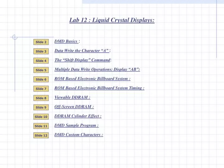
Lab 12 : Liquid Crystal Displays :. DMD Basics :. Slide 2. Data Write the Character “A” :. Slide 3. The “Shift Display” Command :. Slide 4. Multiple Data Write Operations: Display “AB”:. Slide 5. ROM Based Electronic Billboard System :. Slide 6.

E N D
Lab 12 : Liquid Crystal Displays: DMD Basics : Slide 2 Data Write the Character “A” : Slide 3 The “Shift Display” Command: Slide 4 Multiple Data Write Operations: Display “AB”: Slide 5 ROM Based Electronic Billboard System : Slide 6 ROM Based Electronic Billboard System Timing : Slide 7 Viewable DDRAM : Slide 8 Off-Screen DDRAM : Slide 9 DDRAM Cylinder Effect : Slide 10 DMD Sample Program : Slide 11 DMD Custom Characters : Slide 12
W H H W E O E O L R L R L L L L O O D D H E L L H E L W O R L W O R DMD H E W O H H E L H H L E H 0 E L L E L W H Counter ROM W 0 R W W 0 L D R W 0 0 R L W Data ROM Commands Command Register DMD Display H H E E H H E L L E H L L L H O O E L L W W O O W W R O R O W L L R W D D O R L Lab 12 : DMD Basics : Dot Matrix Displays with Hitachi HD44780 controller(or DMD) understand various commands and can easily be programmed to display scrolling messages. Many electronic products use this type of display as an electronic billboard to display messages. H E L L O W O R L D The DMD display can be connected to a ROM. The ROM contains the DMD codes. The counter cycles the address bus to send the codes to the display. H E L L 0 W 0 R L D DMD Display The DMD accepts 2 types of codes. Data codes (ASCII) and command codes (commands like “Shift Message”). The ROM stores a mix of data and commands which makes up the DMD message. Here is the HELLO WORLD sample program. H E L L O W O R L D Initialize the display: Use top line : Auto move cursor. Write next data on the bottom line : Shift the message to the right Shift the message to the right Shift the message to the right Shift the message to the right Shift the message to the right Shift the message to the right Shift the message to the right Slide #2
Data Registers : Display Data RAM : DDRAM 00 0F >Clk Character Generator ROM : CGROM CGRAM Command Register >Clk O1 O0 I0 I1 S S 8 Bit Mux/DeMux I Z 8 Tri-State Buffers HiZ 8 Bit Data Bus E RS R/W DB7 DB0 1 0 0 1 0 0 0 0 0 1 Computer writes code for “A” Lab 12: Data Write Operation: Character “A”: A ROM can be used to send codes to the DMD. However, the DMD was designed to work with a computer system. Let’s look at the computer interface Display the character “A”:Step 1: the computer sends the code 01000001 to the data bus (DB0…DB7). A Step 2: the computer sets R/W (Read Write) to 0. This enables the input buffers and transfers the data bus to MUX. A Step 3: the computer sets RS (Register Select) to 1. This selects channel 1 of Mux/DeMux. The Mux passes the data bus to the CGROM. Step 4: The CGROMretrieves the pixel pattern for character A and gets ready to transfer it to DDRAM. Step 5: The computer provides a clock pulseto the E (enable) input. This clocks the DDRAM registers and completes the write operation. Slide #3
Data Registers : Display Data RAM : DDRAM 00 0F A A >Clk Character Generator ROM : CGROM CGRAM Command Register >Clk O1 O0 I0 I1 S S 8 Bit Mux/DeMux I Z 8 Tri-State Buffers HiZ 8 Bit Data Bus E RS R/W DB7 DB0 0 0 0 0 0 0 0 0 1 1 1 1 1 1 0 0 0 0 Computer writes “Shift Display Right” command Lab 12: Shift Display Command: Let’s assume that the character “A” has been written and is being displayed. We would like to shift the character one position to the right. The DMD has a “Shift Display Right” command. Shift Display Right :Step 1: the computer sends the code 00011100 to the data bus (DB0…DB7). Step 2: the computer sets R/W (Read Write) to 0. This enables the input buffers and transfers the data bus to MUX. Step 3: the computer sets RS (Register Select) to 0. This selects channel 0 of Mux/DeMux. The Mux passes the data bus to the Command Register. Step 4: The computer provides a clock pulseto the E (enable) input. This clock the Command Register and transfers the command. Step 5: The DMD displays executes the shift command. Slide #4
Data Registers : Display Data RAM : DDRAM 00 0F A B >Clk B A Character Generator ROM : CGROM CGRAM Command Register >Clk BF O1 O0 I0 I1 S S 8 Bit Mux/DeMux I Z HiZ 8 Tri-State Buffers HiZ HiZ 8 Bit Data Bus E RS R/W DB7 DB0 1 1 0 1 0 0 BF 0 0 1 1 0 0 1 1 0 0 0 0 0 0 0 0 0 0 0 0 0 0 0 0 1 0 0 0 0 0 1 0 Computer reads the Busy Flag Computer writes code for “A” Computer writes code for “B” Lab 12: Multiple Data Write Operations: Display “AB”: When a computer needs to display a message (more than one character) it must send several data characters one after the other. The computer must give the DMD display enough time to finishone data write operation before it can start another. Display the character “A”:Here are all the steps… A Display the character “B”: Before the “B” character can be displayed the computer must wait until the DMD finishes displaying the letter “A”. The computer must read the DMD Busy Flag (BF). BF=1 means DMD is busy and not ready for a newdata write operation.Here are all the steps… IF BF=1 then the computer must repeat the BF read operation until it finds BF=0. At this time it can proceed with the data write operation of character “B”. Slide #5
Counter ROM DMD Display Lab 12: ROM Based Electronic Billboard System The DMD display was designed to be used with a computer system. The computerwritesdata/command codes and then reads the Busy Flag to see if the DMD is ready for the nextwrite operation. A ROM based system can write data and command codes but it cannot read the Busy Flag! A B 83 milliseconds later To make a ROM based system work it is necessary that the DMD be given enough time to complete a write operation before beginning the nextwrite operation. According to the Hitachi data sheets the slowest write operation takes 1.64 milliseconds. Many other DMD operations execute in microseconds. The ROM based electronic billboard system uses a clock with a clock rate of 12 PPS (or a period of 83 milliseconds). This means that the ROM sends out the code for one write operation and then waits 83 milliseconds to send out the code for the next write operation. At this transfer rate it is NOT necessary to read the Busy Flag and the system works error free! The only disadvantage is that you cannot go any faster than 83 milliseconds per transfer. A computer, on the other hand, can speed up the transfers whenever necessary. This can be useful to give the illusion that an entire word (several characters) can appear on the display at once (instead of 1 character at a time). A computer has more control over the display than a ROM based electronic billboard system. A computer based electronic billboard system is like a car with a variable gas pedal in it. It can go fast or slow whenever necessary. Slide #6
R/W of DMD: The ROM cannot read the Busy Flag. The read mode is not required.Q8 of ROM: Q8=1 for data write and Q8=0 for command write. Q20 of Counter: DMD E requires a negativeedge to complete a write operation. Q20 Q21 Q22 RS=1 Counter Data >Ck Q0 RS=0 Command Q28 Command Register >Ck Q19 E RS DB7 DB6 DB5 DB4 DB3 DB2 DB1 DB0 R/W Q20 >Clk ROM Q8 Q21 A0 25.175 Meg PPS Q7 Q22 A1 Q6 Q23 A2 Q5 Q24 A3 Q4 Q25 A4 Q3 Counter timing diagram. Q26 A5 Q2 Q27 A6 Q1 Q28 A7 Q0 Q29 256X9 Q32 Old 8 bit address New 8 bit address New 8 bit address New Old Lab 12: ROM Based Electronic Billboard System Timing: Q20 frequency = 25.175 Meg PPS/221 = 12.004 PPS Q20 period=1/12.004 =83 milliSec. The counter changes the address of the ROM at every negative edge of Q20 The ROM also changes the data bus at each negative edge of Q20. When the data bus is changing you should NOT clock the DMD (input E). The inverter ensures the DMD is not clocked when the data bus is changing. Here is how it works… The positive edge on Q20 passes through the inverter and becomes a negative edge which clocks the DMD. The DMD is clocked when address and data bus are stable (in the middle of the yellow zone). Slide #7
Viewable : 16 Characters Off-Screen : 24 Characters RS=1 00 01 02 03 04 05 06 07 08 09 0A 0B 0C 0D 0E 0F 10 11 12 13 24 25 26 27 Data >Ck RS=0 Command 40 41 42 43 44 45 46 47 48 49 4A 4B 4C 4D 4E 4F 50 51 52 53 64 65 66 67 Command Register >Ck E RS DB7 DB6 DB5 DB4 DB3 DB2 DB1 DB0 R/W Lab 12: Viewable DDRAM : DDRAM (Display Data RAM) is the memory which stores the data that is viewed by the user of the DMD. It displays 2 lines of 16 characters. It also has 24off-screen characters. The off-screen character will be explained later. DDRAM Add=05 DDRAM Add=45 H e l l o W o r l d Each character position is assigned an address. Line 1 (top) addresses begin at 00HEX and ends at 27HEX. Line 2 (bottom) addresses begin at 40HEX and ends at 67HEX. The addresses are in hex and can easily be converted to binary if you remember: 1 hex numeral = 4 bit binary. To display the word “Hello” in the middle of line 1 you would write the command “Set DDRAM address =05H” and then write the data characters “Hello”. To display the word “World” in the middle of line 2 you would write the command “Set DDRAM address =45H” and then write the data characters “World”. Slide #8
Off-Screen Off-Screen Viewable : 16 Characters Viewable : 16 Characters Viewable : 16 Characters Viewable : 16 Characters Viewable : 16 Characters Viewable : 16 Characters Viewable : 16 Characters Off-Screen : RS=1 00 00 01 01 02 02 03 03 04 04 05 05 06 06 07 07 08 08 09 09 0A 0A 0B 0B 0C 0C 0D 0D 0E 0E 0F 0F 10 10 11 11 12 12 13 13 14 14 15 15 16 16 17 17 Data >Ck RS=0 Command 40 40 41 41 42 42 43 43 44 44 45 45 46 46 47 47 48 48 49 49 4A 4A 4B 4B 4C 4C 4D 4D 4E 4E 4F 4F 50 50 51 51 52 52 53 53 54 54 55 55 56 56 57 57 Command Register >Ck E RS DB7 DB6 DB5 DB4 DB3 DB2 DB1 DB0 R/W H e l l o G o o d W o r l d D a y Lab 12: Off-Screen DDRAM : The off-screenDDRAM characters can be used to store display data and then laterscroll it into view. It is like a holding area for messages. While the userpauses to read the on-screen message the delay can be used to write off-screen. DDRAM Add=40 Shift Display Left Shift Display Left DDRAM Add=50 DDRAM Add=10 DDRAM Add=00 Shift Display Left Shift Display Left Shift Display Left Shift Display Left H e l l o G o o d W o r l d D a y Write the message “Hello World” in the viewable area of the DMD display. Write the message “Good Day” off-screen. The user will see the message “Hello World” and it will seem like the system has paused. The pause is actually the time taken to write “Good Day” off-screen. The “Shift Display Left” command will be used to move the “Good Day” message into view while scrolling “Hello World” out of view. The “Shift Display Left” command moves the messageleftone character position. Five “Shift Display Left” commands are needed to move “Hello World” off screen. The “Shift Display Left” command moves the message to the left but actually moves the Viewable Window to the right. To make the message “Hello World” re-appear you would need to use 5 “Shift Display Right” commands. Slide #9
Viewable : 16 Characters Off-Screen : 24 Characters 00 01 02 03 04 05 06 07 08 09 0A 0B 0C 0D 0E 0F 10 11 12 13 24 25 26 27 D a y G o o d 40 41 42 43 44 45 46 47 48 49 4A 4B 4C 4D 4E 4F 50 51 52 53 64 65 66 67 Viewable Characters! 02 0A 03 09 04 08 05 06 07 G y a 42 o D 4A o d 43 44 49 45 46 47 48 01 09 02 08 03 07 04 05 06 24 41 04 49 25 03 48 42 26 02 47 00 00 04 03 04 43 27 44 00 45 01 46 08 08 0C 0B 0C 01 01 05 04 05 07 07 0B 0B 0A 02 02 05 06 06 06 06 0A 0A 09 03 03 07 07 06 04 04 07 08 08 05 05 09 09 08 64 44 65 43 40 40 43 44 44 66 67 40 41 42 4B 4C 4C 48 48 47 47 41 41 45 45 44 46 46 45 4B 4B 4A 46 46 42 42 43 43 46 47 47 44 44 48 48 47 45 45 49 49 48 49 4A 4A Lab 12: DDRAM Cylinder Effect: DDRAM memory is laid out like a cylinder. Cut out the entire rectangle representing DDRAM and fold it back into a loop. Spin the cylinder and you can see more DDRAM addresses. Spin it more and eventually you reach the last address 27 and 67. 27 and 67 are actually next to 00 and 40 in memory. This means if you write a message off screen at the end of the first line it is next to a message written at address 00. The “Shift Display Right” command can bring both messages into view. Slide #10
Sample Program Address 0 Address 8 RS=1 Counter Data >Ck T T T T e e e s s t Q0 RS=0 Command Command Register 0000 0110 (06) 0000 0001 (01) 0000 1100 (0C) 1100 0000 (C0) 0011 1000 (38) >Ck Q19 E RS DB7 DB6 DB5 DB4 DB3 DB2 DB1 DB0 R/W Q20 ROM >Clk 0 0 1 0 1 0 0 1 1 0 0 038 Q8 Q21 A0 0 0 0 0 1 0 1 0 0 1 1 25.175 Meg PPS 001 Q7 Q22 A1 0 1 1 0 1 0 1 0 0 1 0 1 1 0 0 0 1 0 006 Q6 Q23 A2 0 0 1 0 0 0 0 0 0 0 0 1 0 0 0 0 1 0 00C Q5 Q24 A3 1 1 1 0 1 1 0 0 0 0 1 0 0 0 0 0 0 0 0C0 Q4 Q25 A4 0 0 1 1 0 0 1 0 0 0 0 0 0 0 0 0 1 0 154 Q3 Q26 A5 0 0 0 1 1 0 1 0 0 0 0 0 0 0 0 0 0 0 165 Q2 Q27 A6 0 0 0 0 0 1 0 0 0 0 0 0 0 0 0 0 0 0 0 0 0 0 0 0 0 0 0 0 0 173 Q1 Q28 A7 0 1 1 1 0 1 0 1 1 174 Q0 Q29 0 0 1 0 1 0 0 0 0 0 1 1 0 0 I/D = 1 : Increment the DDRAM address D = 1 : Turn the entire display ON. DL = 1 : Use an 8 bit Data Bus.N = 1 : Use 2 lines of the displayF =0 : 5x7 Dot Matrix Font. Q32 0111 0100 = 74 Hex = “t” (see the CGROM table) 0101 0100 = 54 Hex = “T” (see the CGROM table) 0111 0011 = 73 Hex = “s” (see the CGROM table) 0110 0101 = 65 Hex = “e” (see the CGROM table) C = 0 : Turn the cursor OFF 100 0000 = 40 Hex (Line 2, first position) S = 0 : Move the cursor after data write. Display Freeze B= 0 :DO NOT Blink the character at the cursor position 174 006 173 0C0 038 165 154 001 00C 1 0 0 0 0 1 1 0 1 0 1 0 0 0 0 0 0 0 1 0 1 1 1 0 0 0 1 1 0 1 1 0 0 1 0 0 0 1 1 0 0 0 1 1 0 1 0 0 0 0 1 0 0 0 0 1 1 1 1 0 0 1 0 0 0 0 1 0 0 0 0 1 0 0 1 1 0 0 0 1 0 Set the data write mode 0 0 0 0 0 0 1 I/D S I/D sets the CURSOR/DISPLAY move direction. The CURSOR/DISPLAY will automatically move to the next DDRAM/CGRAM address after each data write. S specifies to shift the display or to move the cursor. CGRAM/DDRAM Data Write CGRAM/DDRAM Data Write CGRAM/DDRAM Data Write CGRAM/DDRAM Data Write Clear Display 1 1 1 1 0 8 bit code for ASCII/JAP/Custom Characters 8 bit code for ASCII/JAP/Custom Characters 8 bit code for ASCII/JAP/Custom Characters 8 bit code for ASCII/JAP/Custom Characters 0 0 0 0 0 0 0 1 Writes data into DDRAM or CGRAM. Used after address has been set. The address pointer is inc/dec automatically. Writes data into DDRAM or CGRAM. Used after address has been set. The address pointer is inc/dec automatically. Writes data into DDRAM or CGRAM. Used after address has been set. The address pointer is inc/dec automatically. Writes data into DDRAM or CGRAM. Used after address has been set. The address pointer is inc/dec automatically. Clears display and returns cursor to home position (DDRAM address = 00H). F * Set DDRAM Address Set Display Mode (Display Function) 0 0 1 0 ADD (7 bit address) 0 1 DL N * Sets the starting DDRAM address. The DDRAMASCII/Jap/Custom characters are sent to this starting address after this setting. DL sets the Data Bus size. N sets the number of lines to be used. F sets the Dot Matrix Font. (1st command) Set Display/Cursor On/Off 0 0 0 0 0 1 D C B D sets display On/Off. C sets cursor On/Off. B enables the character at the cursor position to Blink/Not Blink. Lab 12: DMD Sample Program : The ROM will be loaded with a “Sample Program”. Command Register The counter will start at 0 and cycle forward. Each new count state generates a new address for the ROM and a new code is written to the DMD display. The first 5 codes in ROM (begin with 0xx) are DMD commands they are needed to initialize the display. While these codes are being executed the user will see nothing appear on the display. This initialization sequence is necessary and must be done before the message can be displayed. The last four codes in ROM (begin with 1xx) are ASCII data. They spell out the test message. Slide #11 From DMD command Summary Sheet in Chapter 12.
CGRAM-3 DDRAM RS=1 Data ROM >Ck 058 RS=0 100 Command 10A Command Register 100 >Ck 104 111 10E E RS DB7 DB6 DB5 DB4 DB3 DB2 DB1 DB0 R/W 100 100 0C0 103 1 0 1 1 1 0 1 1 1 1 1 0 0 0 0 0 0 0 0 0 1 0 0 0 1 0 0 0 1 0 0 0 0 0 0 0 0 0 0 0 0 0 0 0 0 0 0 0 0 0 1 0 1 0 0 0 0 1 0 0 0 0 0 1 1 0 0 1 0 0 1 0 0 0 0 0 0 0 0 0 1 1 0 0 1 0 0 0 0 0 0 0 0 0 0 0 0 1 1 Cursor row 5 Pixels Lab 12: DMD Custom Characters : Custom characters are user defined. DMD displays have 8 custom characters. A custom character is initialized once and then accessed as many times as necessary. A happy face character will be created and displayed. 01 01 1000 Set CGRAM-3 1 100 0000 DDRAM add. =40 Step 1: The face will be saved into CGRAM-3. Use the “CGRAM Address Set” command to inform the DMD display that the next data transfers are pixel layouts that belong in CGRAM. This command prevents the DMD from transferring the data to DDRAM as ASCII data. CGRAM Address Set = 058 = 01 01 1000 (6 bit address is 18 hex for CG3). Step 2: Use data write operations to fill in the pixel layout of the happy face. Remember each row is made up of 5 dots(pixels). The character is made up of 7 rows (+ 1 cursor row) of 5 pixels. It will take 8 data write operations to define the face. Remember data writes now go to CGRAM. Logic 0 = pixel offLogic 1 = pixel on Step 3: To access the character you must issue a DDRAM Address Set command. This will cause subsequent data transfers to be sent to DDRAM and stop data transfers to CGRAM. The face character can be accessed at address 03 (see chapter 12 for details). We will display it on the bottom line. Slide #12